AD9822 데이터 시트보기 (PDF) - Analog Devices
부품명
상세내역
제조사
AD9822 Datasheet PDF : 20 Pages
| |||
AD9822
Parameter
POWER DISSIPATION
3-Channel Mode
3-Channel Mode @ 6 MHz
1-Channel Mode
1-Channel Mode @ 6 MHz
Min
Typ
385
335
300
250
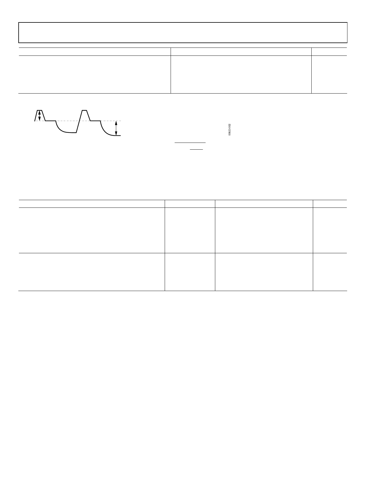
1 Linear input signal range is from 2 V to 4 V when the CCD’s reference level is clamped to 4 V by the AD9822’s input clamp.
Max
450
410
1V TYP
RESET TRANSIENT
4V SET BY INPUT CLAMP (3V OPTION ALSO AVAILABLE)
2V p-p MAX INPUT SIGNAL RANGE
[ 2 The PGA gain is approximately linear-in-dB and follows the equation: Gain =
5.7
] where G is the register value. See Figure 15.
⎡ 63 − G ⎤
1 + 4.7 ⎢
⎣
63
⎥
⎦
Unit
mW
mW
mW
mW
DIGITAL SPECIFICATIONS
TMIN to TMAX, AVDD = 5 V, DRVDD = 5 V, CDS mode, fADCCLK = 15 MHz, fCDSCLK1 = fCDSCLK2 = 5 MHz, CL = 10 pF, unless otherwise noted.
Table 2.
Parameter
LOGIC INPUTS
High Level Input Voltage
Low Level Input Voltage
High Level Input Current
Low Level Input Current
Input Capacitance
LOGIC OUTPUTS
High Level Output Voltage
Low Level Output Voltage
High Level Output Current
Low Level Output Current
Symbol
VIH
VIL
IIH
IIL
CIN
VOH
VOL
IOH
IOL
Min
Typ
Max
Unit
2.0
V
0.8
V
10
µA
10
µA
10
pF
4.5
V
0.1
V
50
µA
50
µA
Rev. B | Page 4 of 20
Share Link: 