TSV914ID 데이터 시트보기 (PDF) - STMicroelectronics
부품명
상세내역
제조사
TSV914ID Datasheet PDF : 18 Pages
| |||
TSV911-TSV912-TSV914
Electrical characteristics
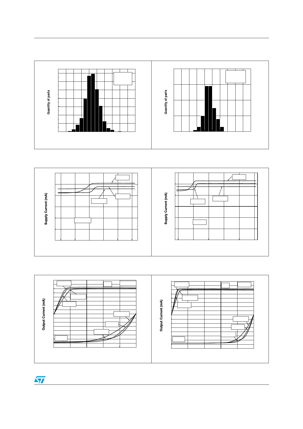
Figure 1. Input offset voltage distribution at Figure 2. Input offset voltage distribution at
T=25°C
T=125°C
140
Vcc=5V
Vicm=2.5V
120
Tamb=25°C
100
80
60
40
20
0
-5 -4 -3 -2 -1 0 1 2 3 4 5
Input offset Voltage (mV)
40
Vcc=5V
Vicm=2.5V
Tamb=125°C
30
20
10
0
-5 -4 -3 -2 -1 0 1 2 3 4 5
Input offset Voltage (mV)
Figure 3.
1.0
0.8
Supply current vs. input common
mode voltage at Vcc=2.5V
° T=25 C
Figure 4.
1.0
0.8
Supply current vs. input common
mode voltage at Vcc=5V
° T=25 C
0.7
T=-40°C
° T=125 C
0.5
0.7
T=-40°C
° T=125 C
0.5
0.3
Vcc=2.5V
0.2
0.3
Vcc=5V
0.2
0.0
0.0
0.5
1.0
1.5
2.0
Input Common Mode Voltage (V)
2.5
0.0
0
1
2
3
4
5
Input Common Mode Voltage (V)
Figure 5. Output current vs. output voltage at Figure 6. Output current vs. output voltage at
Vcc=2.5V
Vcc=5V
40
35 T=-40°C
30
Sink
Vcc=2.5V
25
20
° T=125 C
15
10
° T=25 C
5
0
° T=125 C
-5
-10
-15
-20
-25
-30 Source
° T=25 C
T=-40°C
-35
-40
0.0
0.5
1.0
1.5
2.0
2.5
Output Voltage (V)
40
35 T=-40°C
30
Sink
Vcc=5V
25
20
° T=125 C
15
10
° T=25 C
5
0
-5
-10
-15
-20
-25
-30 Source
° T=125 C
° T=25 C
T=-40°C
-35
-40
0.0
1.0
2.0
3.0
4.0
5.0
Output Voltage (V)
9/18
Share Link: 