U2010B-XFP 데이터 시트보기 (PDF) - Atmel Corporation
부품명
상세내역
제조사
U2010B-XFP Datasheet PDF : 13 Pages
| |||
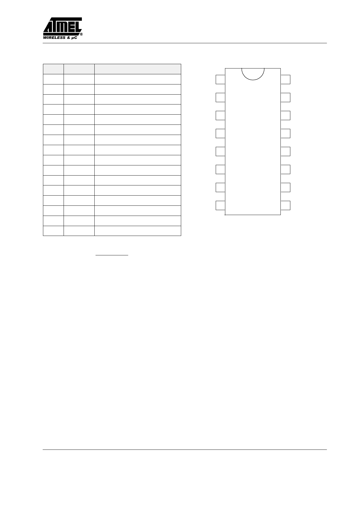
U2010B
Pin Description
Pin Symbol
Function
1
Isense Load current sensing
2
Isense Load current sensing
3
Cö Ramp voltage
4 Control Control input
5
Comp. Compensation output
6
ILoad Load current limitation
7
Csoft Soft start
8
VRef Reference voltage
9
Mode Mode selection
10
GND Ground
11
VS Supply voltage
12 High load High load indication
13 Overload Overload indication
14
VRö Ramp current adjust
15
VSync. Voltage synchronization
16 Output Trigger output
Series resistance R1 can be calculated as follows:
R 1max
+
Vmains
2
–
VSmax
I tot
where:
Vmains
VSmax
Itot
ISmax
Ix
+ Mains supply voltage
+ Maximum supply voltage
+ Total current consumption = ISmax )Ix
+ Maximum current consumption of the IC
+ Current consumption of the
external components
Voltage Monitoring
When the voltage is built up, uncontrolled output pulses
are avoided by internal voltage monitoring. Apart from
that, all latches in the circuit (phase control, load limit
regulation) are reset and the soft-start capacitor is short
circuited. This guarantees a specified start-up behavior
each time the supply voltage is switched on or after short
interruptions of the mains supply. Soft start is initiated
after the supply voltage has been built up. This behavior
guarantees a gentle start-up for the motor and auto-
matically ensures the optimum run-up time.
Phase Control
The function of the phase control is largely identical to the
well-known IC U211B. The phase angle of the trigger
pulse is derived by comparing the ramp voltage V3 which
is mains-synchronized by the voltage detector with the set
Isense 1
Isense 2
Cö 3
Control 4
Comp. 5
ILoad 6
Csoft 7
VRef 8
U2010B
16 Output
15 VSync.
14 VRö
13 Overload
12 High load
11 VS
10 GND
9 Mode
Figure 3. Pinning
value on the control input, Pin 4. The slope of the ramp
is determined by Cö and its charging current Iö. The
charging current can be varied using Rö at Pin 14. The
maximum phase angle, αmax, can also be adjusted by
using Rö (minimum current flow angle ömin), see
figure 5.
When the potential on Pin 3 reaches the set point level of
Pin 4, a trigger pulse width, tp, is determined from the
value of Cö (tp = 9 ms/nF). At the same time, a latch is set
with the output pulse, as long as the automatic
retriggering has not been activated, then no more pulses
can be generated in that half cycle. Control input at Pin 4
(with respect to Pin 10) has an active range from
V8 to –1 V. When V4 = V8, then the phase angle is at its
maximum, αmax, i.e., the current flow angle is minimum.
The minimum phase angle, αmin, is set with V4 w –1 V.
Automatic Retriggering
The current-detector circuit monitors the state of the triac
after triggering by measuring the voltage drop at the triac
gate. A current flow through the triac is recognized when
the voltage drop exceeds a threshold level of typ. 40 mV.
If the triac is quenched within the relevant half-wave after
triggering (for example owing to low load currents before
or after the zero crossing of current wave, or for commu-
tator motors, owing to brush lifters), the automatic
retriggering circuit ensures immediate retriggering, if
Rev. A4, 23-Nov-00
3 (13)
Share Link: 