AT6000 데이터 시트보기 (PDF) - Atmel Corporation
부품명
상세내역
제조사
AT6000 Datasheet PDF : 28 Pages
| |||
AT6000(LV) Series
Clock Distribution
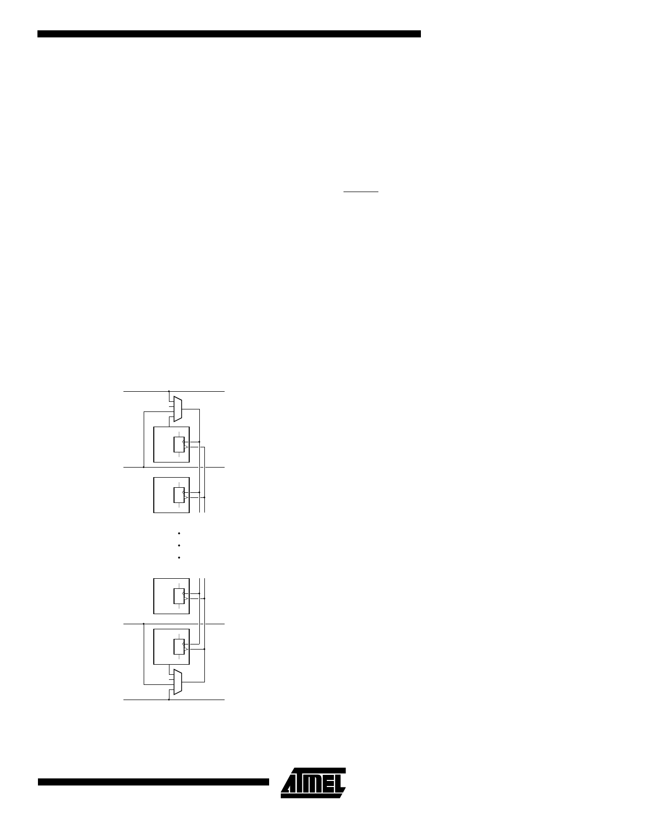
Along the top edge of the array is logic for distributing clock
signals to the D flip-flop in each logic cell (Figure 10). The
distribution network is organized by column and permits
columns of cells to be independently clocked. At the head
of each column is a user-configurable multiplexer providing
the clock signal for that column. It has four inputs:
• Global clock supplied through the CLOCK pin
• Express bus adjacent to the distribution logic
• “A” output of the cell at the head of the column
• Logical constant “1” to conserve power (no clock)
Through the global clock, the network provides low-skew
distribution of an externally supplied clock to any or all of
the columns of the array. The global clock pin is also con-
nected directly to the array via the A input of the upper left
and right corner cells (AW on the left, and AN on the right).
The express bus is useful in distributing a secondary clock
to multiple columns when the global clock line is used as a
primary clock. The A output of a cell is useful in providing a
clock signal to a single column. The constant “1” is used to
reduce power dissipation in columns using no registers.
Figure 10. Column Clock and Column Reset
GLOBAL
CLOCK
"1"
GLOBAL
CLOCK
EXPRESS
BUS
EXPRESS
BUS
GLOBAL
RESET
A
D
Q
CELL
D
Q
CELL
CELL
D
Q
CELL
D
Q
A
"1"
EXPRESS
BUS
D
E
D
I
C
A
T
E
B
U
R
I
E
D
R
O
U
T
I
N
G
D
EXPRESS
BUS
GLOBAL
RESET
Asynchronous Reset
Along the bottom edge of the array is logic for asynchro-
nously resetting the D flip-flops in the logic cells
(Figure 10). Like the clock network, the asynchronous reset
network is organized by column and permits columns to be
independently reset. At the bottom of each column is a
user-configurable multiplexer providing the reset signal for
that column. It has four inputs:
• Global asynchronous reset supplied through the
RESET pin
• Express bus adjacent to the distribution logic
• “A” output of the cell at the foot of the column
• Logical constant “1” to conserve power
The asynchronous reset logic uses these four inputs in the
same way that the clock distribution logic does. Through
the global asynchronous reset, any or all columns can be
reset by an externally supplied signal. The global asynchro-
nous reset pin is also connected directly to the array via the
A input of the lower left and right corner cells (AS on the
left, and AE on the right). The express bus can be used to
distribute a secondary reset to multiple columns when the
global reset line is used as a primary reset, the A output of
a cell can also provide an asynchronous reset signal to a
single column, and the constant “1” is used by columns
with registers requiring no reset. All registers are reset dur-
ing power-up.
Input/Output
The Atmel architecture provides a flexible interface
between the logic array, the configuration control logic and
the I/O pins.
Two adjacent cells – an “exit” and an “entrance” cell – on
the perimeter of the logic array are associated with each
I/O pin.
There are two types of I/Os: A-type (Figure 11) and B-type
(Figure 12). For A-type I/Os, the edge-facing A output of an
exit cell is connected to an output driver, and the edge-
facing A input of the adjacent entrance cell is connected to
an input buffer. The output of the output driver and the input
of the input buffer are connected to a common pin.
B-type I/Os are the same as A-type I/Os, but use the B
inputs and outputs of their respective entrance and exit
cells. A- and B-type I/Os alternate around the array Control
of the I/O logic is provided by user-configurable memory
bits.
7
Share Link: 