MC33030P 데이터 시트보기 (PDF) - Motorola => Freescale
부품명
상세내역
제조사
MC33030P Datasheet PDF : 16 Pages
| |||
MC33030
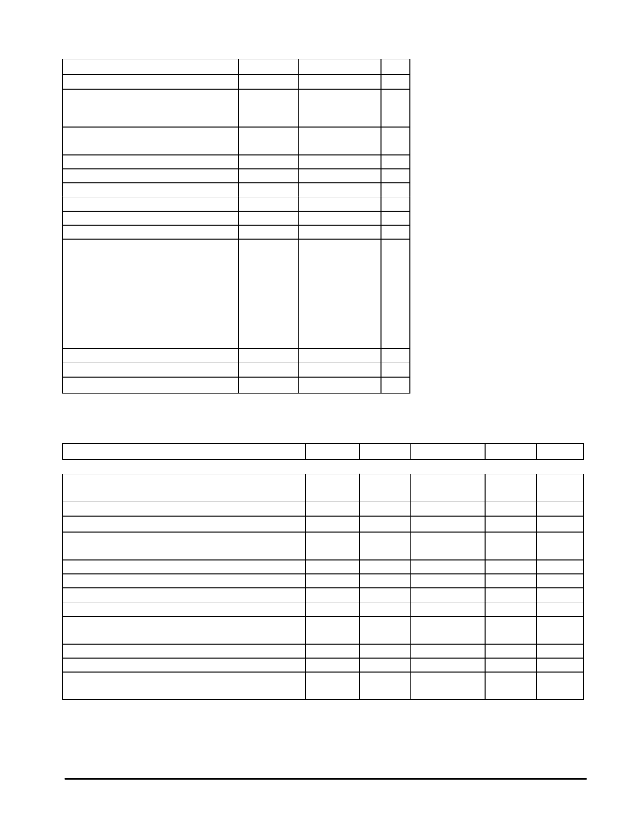
MAXIMUM RATINGS
Rating
Power Supply Voltage
Input Voltage Range
Op Amp, Comparator, Current Limit
(Pins 1, 2, 3, 6, 7, 8, 9, 15)
Symbol
VCC
VIR
Value
Unit
36
V
– 0.3 to VCC
V
Input Differential Voltage Range
Op Amp, Comparator (Pins 1, 2, 3, 6, 7, 8, 9)
VIDR
– 0.3 to VCC
V
Delay Pin Sink Current (Pin 16)
Output Source Current (Op Amp)
Drive Output Voltage Range (Note 1)
Drive Output Source Current (Note 2)
Drive Output Sink Current (Note 2)
Brake Diode Forward Current (Note 2)
Power Dissipation and Thermal
Characteristics
P Suffix, Dual In Line Case 648C
Thermal Resistance, Junction–to–Air
Thermal Resistance, Junction–to–Case
(Pins 4, 5, 12, 13)
DW Suffix, Dual In Line Case 751G
Thermal Resistance, Junction–to–Air
Thermal Resistance, Junction–to–Case
(Pins 4, 5, 12, 13)
IDLY(sink)
Isource
VDRV
IDRV(source)
IDRV(sink)
IF
20
10
– 0.3 to (VCC + VF)
1.0
1.0
1.0
RθJA
80
RθJC
15
RθJA
94
RθJC
18
mA
mA
V
A
A
A
°C/W
Operating Junction Temperature
Operating Ambient Temperature Range
Storage Temperature Range
TJ
+150
°C
TA
– 40 to + 85
°C
Tstg
– 65 to +150
°C
NOTES: 1. The upper voltage level is clamped by the forward drop, VF, of the brake diode.
2. These values are for continuous DC current. Maximum package power dissipation limits must
be observed.
ELECTRICAL CHARACTERISTICS (VCC = 14 V, TA = 25°C, unless otherwise noted.)
Characteristic
Symbol
Min
Typ
Max
ERROR AMP
p p Input Offset Voltage (– 40°C TA 85°C)
VPin 6 = 7.0 V, RL = 100 k
VIO
–
1.5
10
Input Offset Current (VPin 6 = 1.0 V, RL = 100 k)
Input Bias Current (VPin 6 = 7.0 V, RL = 100 k)
Input Common–Mode Voltage Range
∆VIO = 20 mV, RL = 100 k
IIO
IIB
VICR
–
0.7
–
–
7.0
–
–
0 to (VCC – 1.2)
–
Slew Rate, Open Loop (VID = 0.5 V, CL = 15 pF)
Unity–Gain Crossover Frequency
Unity–Gain Phase Margin
SR
–
0.40
–
fc
–
550
–
φm
–
63
–
Common–Mode Rejection Ratio (VPin 6 = 7.0 V, RL = 100 k)
CMRR
50
82
–
Power Supply Rejection Ratio
VCC = 9.0 to 16 V, VPin 6 = 7.0 V, RL = 100 k
PSRR
–
89
–
Output Source Current (VPin 6 = 12 V)
Output Sink Current (VPin 6 = 1.0 V)
Output Voltage Swing (RL = 17 k to Ground)
IO +
–
1.8
–
IO –
–
250
–
VOH
12.5
13.1
–
VOL
–
0.02
–
NOTES: 3. The upper or lower hysteresis will be lost when operating the Input, Pin 3, close to the respective rail. Refer to Figure 4.
4. Low duty cycle pulse techniques are used during test to maintain junction temperature as close to ambient temperature as possible.
Unit
mV
nA
nA
V
V/µs
kHz
deg.
dB
dB
mA
µA
V
V
2
MOTOROLA ANALOG IC DEVICE DATA
Share Link: 