UPD160040 데이터 시트보기 (PDF) - NEC => Renesas Technology
부품명
상세내역
제조사
UPD160040
NEC => Renesas Technology

UPD160040 Datasheet PDF : 19 Pages
| |||
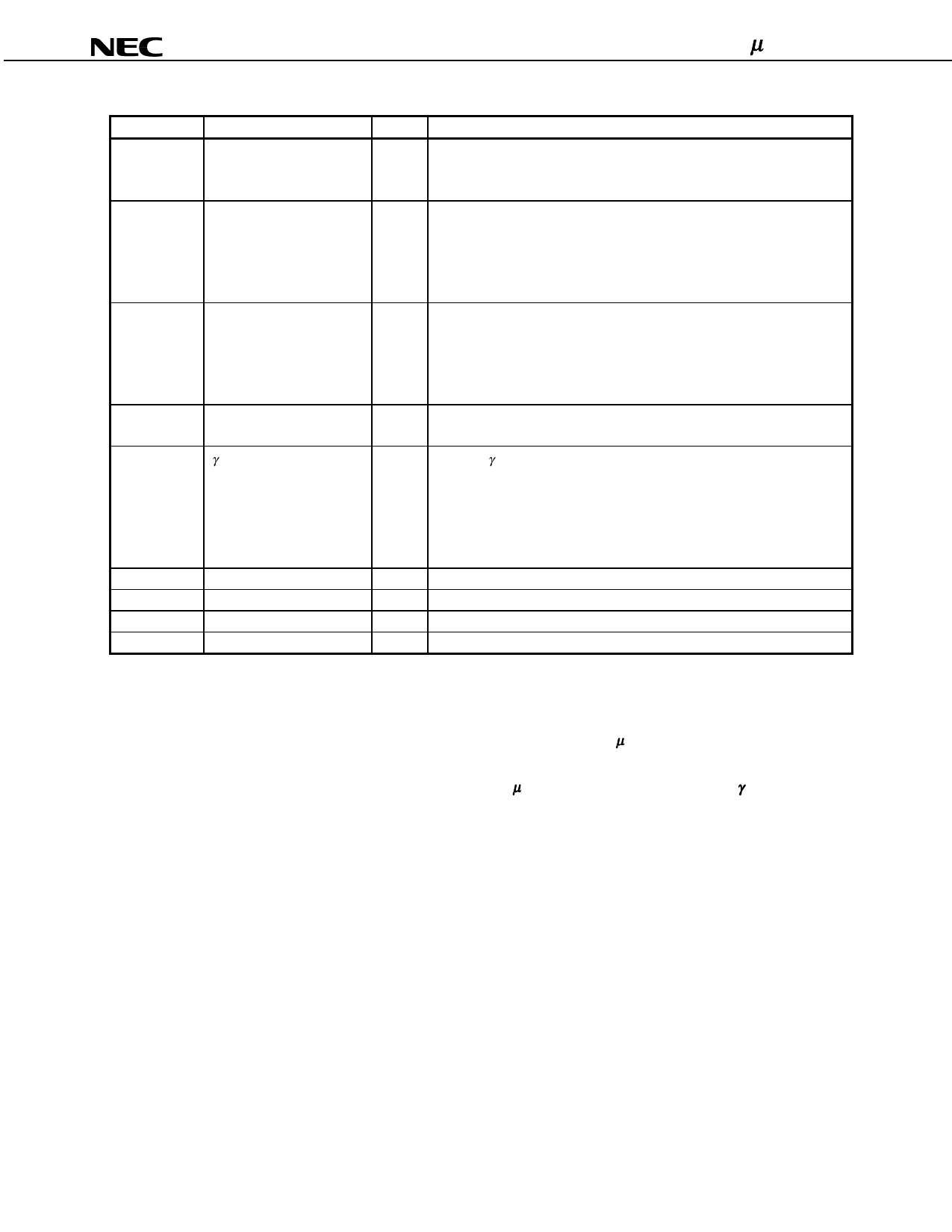
µPD160040
Pin Symbol
MODE
POL21,
POL22
VSEL
TEST
V0-V15
VDD1
VDD2
VSS1
VSS2
Pin Name
Output reset control
Data inversion
Driver voltage select
Test
γ -corrected power supplies
Logic power supply
Driver power supply
Logic ground
Driver ground
I/O
Input
Input
Input
Input
−
−
−
−
−
(2/2)
Description
MODE = H or open: Output reset
MODE = L: No output reset
MODE is pulled up to the VDD1 in the IC.
Select of inversion or no inversion for input data.
POL21: Data inversion or no inversion of Port1.
POL22: Data inversion or no inversion of Port2
POL21, POL22 = H: Data are inverted in the IC.
POL21, POL22 = L: Data are not inverted in the IC.
The driver voltage can be switched by controlling the stationary bias
current of the output amplifier via VSEL.
VSEL = H: VDD2 = 12.5 to (14.0 V) (large bias current)
VSEL = L or open: VDD2 = (14.0 V) to 15.0 V (small bias current)
LPC is pulled down to the VSS1 in the IC.
Normally, set the TEST pin to H or leave open.
This pin is pulled up to VDD1 in the IC.
Input the γ -corrected power supplies from outside by using operational
amplifier. During the gray scale voltage output, be sure to keep the gray
scale level power supply at a constant level. Make sure to maintain the
following relationships.
VDD2 – 0.2 V ≥ V0 > V1 > V2 > V1 > V2 >... ... > V6 > V7 ≥ 0.5 VDD2 + 0.5 V
0.5 VDD2 – 0.5 V ≥ V8 > V9 > V10 > ... ... > V14 > V15 ≥ VSS2 + 0.2 V
2.5 to 3.6 V
12.5 to 15.5 V
Grounding
Grounding
Cautions 1. The power start sequence must be VDD1, logic input, and VDD2 & V0-V15 in that order.
Reverse this sequence to shut down.
2. To stabilize the supply voltage, please be sure to insert a 0.47 µF bypass capacitor between
VDD1-VSS1 and VDD2-VSS2. Furthermore, for increased precision of the D/A converter,
insertion of a bypass capacitor of about 0.1 µF is also advised between the γ-corrected
power supply terminals (V0, V1, V2,.. ..., V15) and VSS2.
Data Sheet S15859EJ1V0DS
5
Share Link: