UPD160061A 데이터 시트보기 (PDF) - NEC => Renesas Technology
부품명
상세내역
제조사
UPD160061A
NEC => Renesas Technology

UPD160061A Datasheet PDF : 18 Pages
| |||
µPD160061A
5. RELATIONSHIP BETWEEN INPUT DATA AND OUTPUT VOLTAGE VALUE
The µPD160061A incorporates a 6-bit D/A converter whose odd output pins and even output pins output respectively
gray scale voltages of differing polarity with respect to the LCD’s counter electrode voltage. The D/A converter consists of
ladder resistors and switches.
The ladder resistors (r0 to r62) are designed so that the ratio of LCD panel γ-compensated voltages to V0’ to V63’ and V0”
to V63” is almost equivalent, resistor ratio is shown in Figure 5−2. For the 2 sets of five γ-compensated power supplies, V0
to V4 and V5 to V9, respectively, input gray scale voltages of the same polarity with respect to the common voltage. When
fine-gray scale voltage precision is not necessary, there is no need to connect a voltage follower circuit to the γ-
compensated power supplies V1 to V3 and V6 to V8.
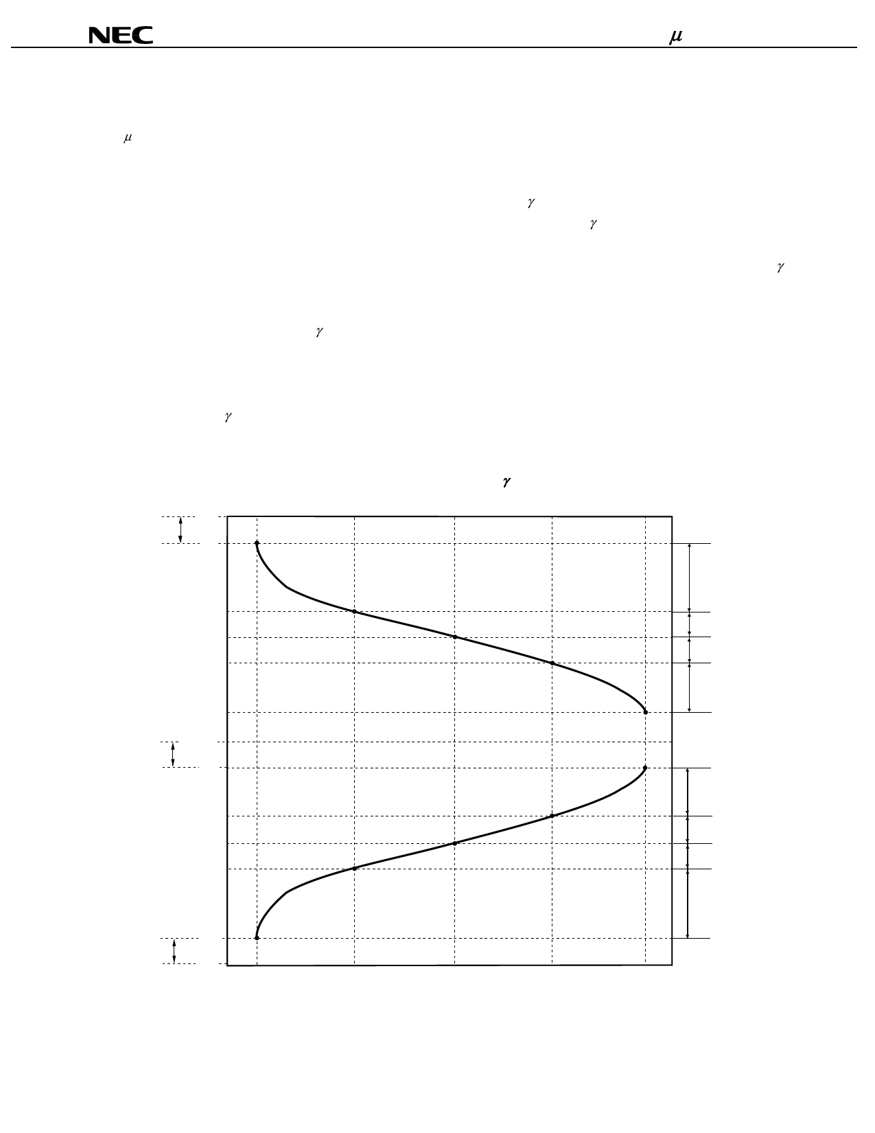
Figure 5–1 shows the relationship between the driving voltages such as liquid-crystal driving voltages VDD2 and VSS2,
common electrode potential VCOM, and γ -corrected voltages V0 to V9 and the input data. Be sure to maintain the voltage
relationships of below.
VDD2 – 0.2 V ≥ V0 > V1 > V2 > V3 > V4 ≥ 0.5 VDD2
0.5 VDD2 – 0.3 V ≥ V5 > V6 > V7 > V8 > V9 > VSS2 + 0.2 V
Figures 5–2 indicates γ -corrected voltages and ladder resistors ratio. Figures 5–3 indicates the relationship between the
input data and output voltage.
Figure 5–1. Relationship between Input Data and γ - corrected Power Supplies
0.2 V
VDD2
V0
V1
V2
V3
V4
0.3 V
0.5 VDD2
V5
V6
V7
V8
16
16
16
16
Split interval
16
16
16
V9
0.2 V
VSS2
00
10
20
30
Input data (HEX.)
16
3F
6
Data Sheet S16041EJ2V0DS
Share Link: