UPD16650N 데이터 시트보기 (PDF) - NEC => Renesas Technology
부품명
상세내역
제조사
UPD16650N Datasheet PDF : 12 Pages
| |||
µPD16650
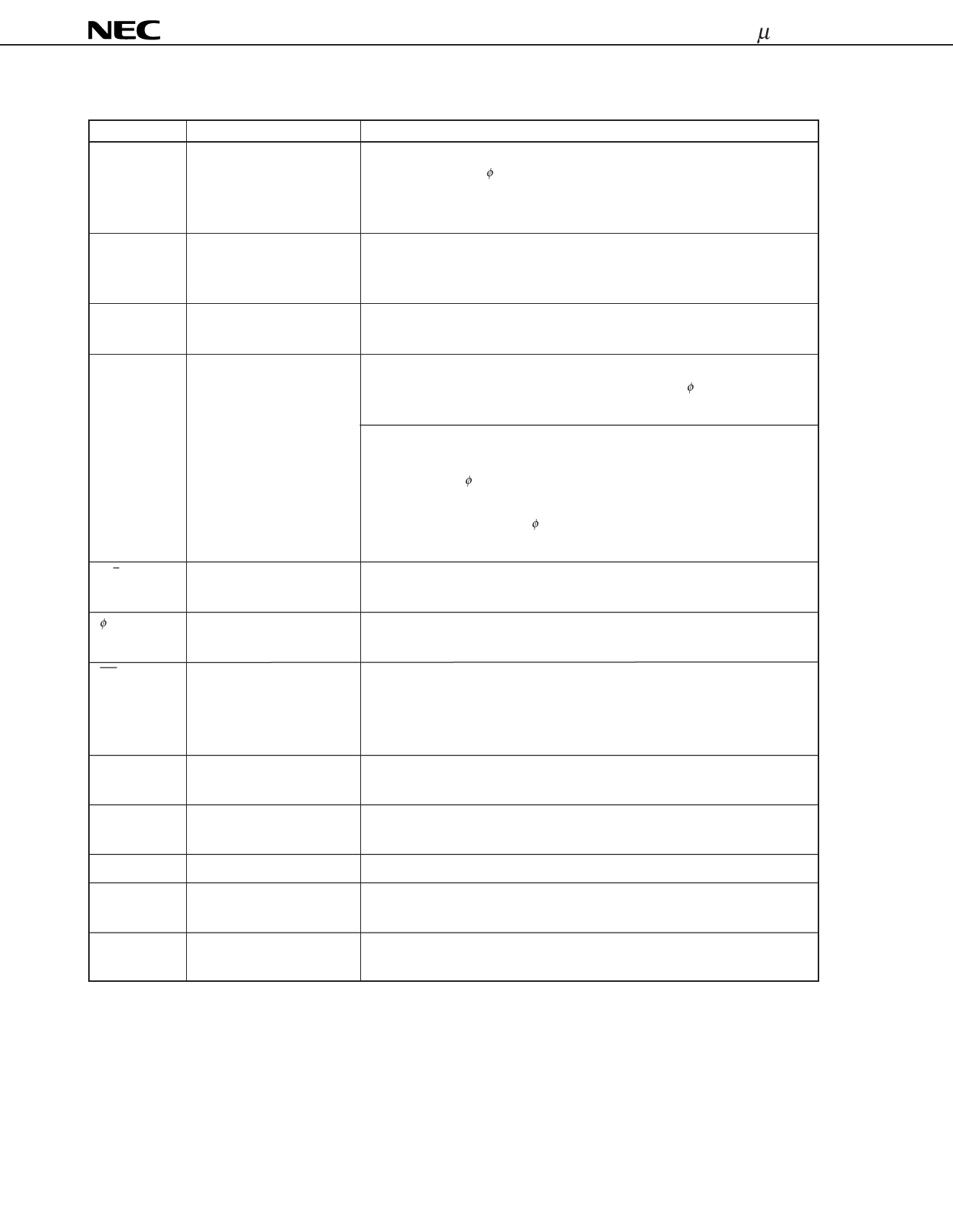
PIN DESCRIPTION
Pin symbol
X1 to X128
MC
VCHA
STVR
STVL
R/L
φX
OE
VDD
VCC
VSS
VEE1
VEE2
Pin name
Driver output
Description of function
Output scan signals to drive the TFT-LCD gate electrodes. The output changes
when the shift clock φX rises. The amplitude of the driver output is VDD - VEE1.
See the timing charts shown later for details of how to switch between the 120-
output mode and 128-output mode.
Output count change-over
input
Receives a signal that changes the number of outputs. For the 120-output
mode, this pin must be supplied with a high level (VCC). For the 128-output
mode, it must be supplied with a low level (VSS or VEE2).
Logic voltage change-over Must be supplied with the VEE2 level when the logic supply voltage is 3.3 V, and
input
with the VDD level when the logic supply voltage is 5.0 V.
Start pulse input/output
Receives an input to the internal shift register. The input data is loaded on the
shift register at the positive-going edge of the shift clock φX. The scan signals
are output from X1 to X128. The input/output level is the CMOS level.
Outputs a start pulse to the next stage if a cascade connection is used. In the
120-output mode, the start pulse is output at the negative-going edge of the
120th shift clock φX pulse, and cleared at the negative-going edge of the 121st
pulse. In the 128-output mode, the start pulse is output at the negative-going
edge of the 128th shift clock φX pulse, and cleared at the negative-going edge
of the 129th pulse.
Shift direction change-over R/L = high (for shift right): STVR → X1 → X128 → STVL
input
R/L = low (for shift left) : STVL → X128 → X1 → STVR
Shift clock input
Receives a shift clock pulse for the internal shift register. A shift occurs at the
positive-going edge of the shift clock pulse.
Output enable input
When this pin is at a high level, the driver output is fixed at a low level. The
shift register is not cleared, however. The internal logic circuit operates even
when the pin is at a high level. The signal supplied to this pin is not
synchronized with the clock.
Driver positive supply volt- Receives the supply voltage for both the logic circuit and driver.
age
Reference voltage
5 ±0.5 V/3.3 ±0.3 V
Reference voltage for the LS1 and LS2 level shifters.
Ground
Must be connected to the system ground.
Driver negative supply volt- VEE1 (for the driver)
age
Driver negative supply volt- VEE2 (for the logic circuit)
age
4
Share Link: 