UPD16641N 데이터 시트보기 (PDF) - NEC => Renesas Technology
부품명
상세내역
제조사
UPD16641N Datasheet PDF : 20 Pages
| |||
µPD16641
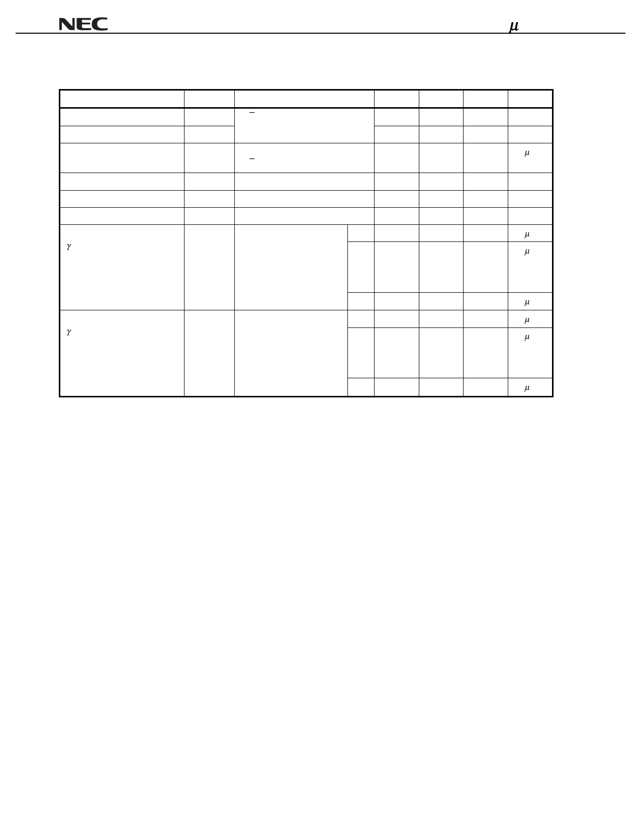
Electrical Characteristics (TA = –10 to +75°C, VDD1 = 3.0 to 3.6 V, VDD2 = 3.0 to 3.6 V or 4.5 to 5.5 V, VSS1 = VSS2 = 0 V)
Parameter
Symbol
Condition
MIN.
TYP.
MAX.
Unit
High-level input voltage
Low-level input voltage
VIH
R/L, CLK, STB, STHR (L),
VIL
D00-05, D10-15, D20-25
0.7VDD1
0
VDD1
V
0.3VDD1
V
Input leakage current
IL
D00-05, D10-15, D20-25
R/L, CLK, STB, STHR (L)
±1.0
µA
Pull-up resistor
RPU
Vsel, VDD2 = 5.0 V, Vsel, = 0 V
40
100
250
kΩ
High-level output voltage
VOH
STHR (L), IO = –1.0 mA
VDD1 – 0.5
V
Low-level output voltage
VOL
STHR (L), IO = +1.0 mA
0.5
V
Static current consumption of
IVn1
VDD1 = 3.3 V, VDD2 = 3.3 V
V10
–200
–150
µA
γ-corrected power (VDD2 = 3.3 V)
V0 = 3.20 V, V6 = 1.95 V
V1 = 3.07 V, V7 = 1.70 V
V9
±10
µA
V2 = 2.80 V, V8 = 1.46 V
to
V3 = 2.57 V, V9 = 1.11 V
V1
V4 = 2.34 V, V10 = 0.10 V
V5 = 2.12 V,Note
V0
150
200
µA
Static current consumption of
IVn2
VDD1 = 3.3 V, VDD2 = 5.0 V
V10
–300
–250
µA
γ-corrected power (VDD2 = 5.0 V)
V0 = 4.90 V, V6 = 2.96 V
V1 = 4.69 V, V7 = 2.58 V
V9
±10
µA
V2 = 4.28 V, V8 = 2.20 V
to
V3 = 3.92 V, V9 = 1.66 V
V1
V4 = 3.56 V, V10 = 0.1 V
V5 = 3.23 V,Note
V0
250
300
µA
(VX is output voltage of analog output pin S1 to S240. VOUT is the voltage applied to analog output pin S1 to S240.)
Note Apply ideal voltage to V1 to V9 that is calculated from internal resistor.
10
Share Link: 