UPD16641N 데이터 시트보기 (PDF) - NEC => Renesas Technology
부품명
상세내역
제조사
UPD16641N Datasheet PDF : 20 Pages
| |||
µPD16641
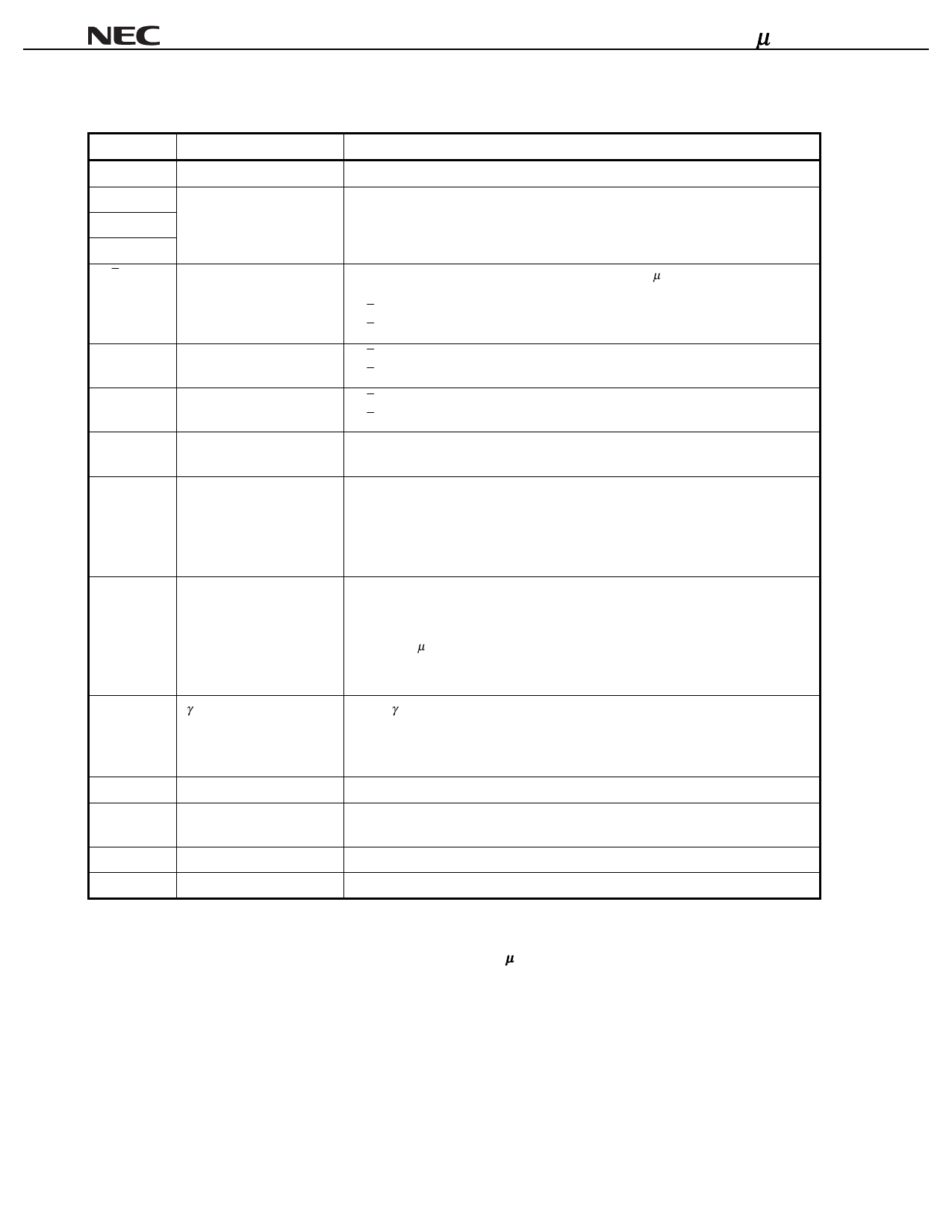
3. PIN DESCRIPTION
Pin Symbol
S1 to S240
D00 to D05
D10 to D15
D20 to D25
R/L
STHR
STHL
Vsel
CLK
STB
V0 to V10
VDD1
VDD2
VSS1
VSS2
Pin Name
Driver output
Display data input
Shift direction select input
Right shift start pulse I/O
Left shift start pulse I/O
Driver voltage selection
Shift clock input
Latch input
γ-corrected power supply
Logic circuit power supply
Driver circuit power supply
Logic ground
Driver ground
Description
Output 64 gray scale analog voltages converted from digital signals.
Inputs 18-bit-wide display gray scale data (6 bits) × 3 dots (RGB).
DX0: LSB, DX5: MSB
This pin inputs/outputs start pulses when two or more µPD16641s are connected
in cascade. Shift direction of shift register is as follows:
R/L = H : STHR input, S1 → S240, STHL output
R/L = L : STHL input, S240 → S1, STHR output
R/L = H : Inputs start pulse.
R/L = L : Outputs start pulse.
R/L = H : Outputs start pulse.
R/L = L : Inputs start pulse.
Selects driver voltage. This pin is internally pulled up to VDD2.
Vsel = VDD2 or OPEN: VDD2 = 3.3 V ± 0.3 V, Vsel = L: VDD2 = 5.0 V ± 0.5 V
Inputs shift clock to shift register. Display data is loaded to data register at rising
edge of this pin.
Start pulse output goes high at rising edge of 80th clock after start pulse has been
input, and serves as start pulse to driver in next stage. 80th clock of driver in first
stage serves as start pulse of driver in next stage.
Contents of data register are latched at rising edge, transferred to D/A converter,
and output as analog voltage corresponding to display data. Contents of initial
shift register are cleared after STB has been input. One pulse of this signal is
input when µPD16641 is started, and then device operates normally. For STB
input timing, refer to Relations between STB, Start Pulse, and Blanking Period
in Switching Characteristic Waveform.
Inputs γ-corrected power from external source.
VSS2 ≤ V10 ≤ V9 ≤ V8 ≤ V7 ≤ V6 ≤ V5 ≤ V4 ≤ V3 ≤ V2 ≤ V1 ≤ V0 ≤ VDD2
VSS2 ≤ V0 ≤ V1 ≤ V2 ≤ V3 ≤ V4 ≤ V5 ≤ V6 ≤ V7 ≤ V8 ≤ V9 ≤ V10 ≤ VDD2
Maintain gray scale power supply during gray scale voltage output.
3.3 V ± 0.3 V
Vsel = VDD2 or OPEN : VDD2 = 3.3 V ± 0.3 V
Vsel = L
: VDD2 = 5.0 V ± 0.5 V
Ground
Ground
Caution Be sure to turn on power in the order VDD1, logic input, VDD2, and gray scale power (V0 to V10), and
turn off power in the reverse order, to prevent the µPD16641 from being damaged by latchup. Be
sure to observe this power sequence even during a transition period.
4
Share Link: 