UPD161602AP 데이터 시트보기 (PDF) - NEC => Renesas Technology
부품명
상세내역
제조사
UPD161602AP
NEC => Renesas Technology

UPD161602AP Datasheet PDF : 23 Pages
| |||
µPD161602A/B
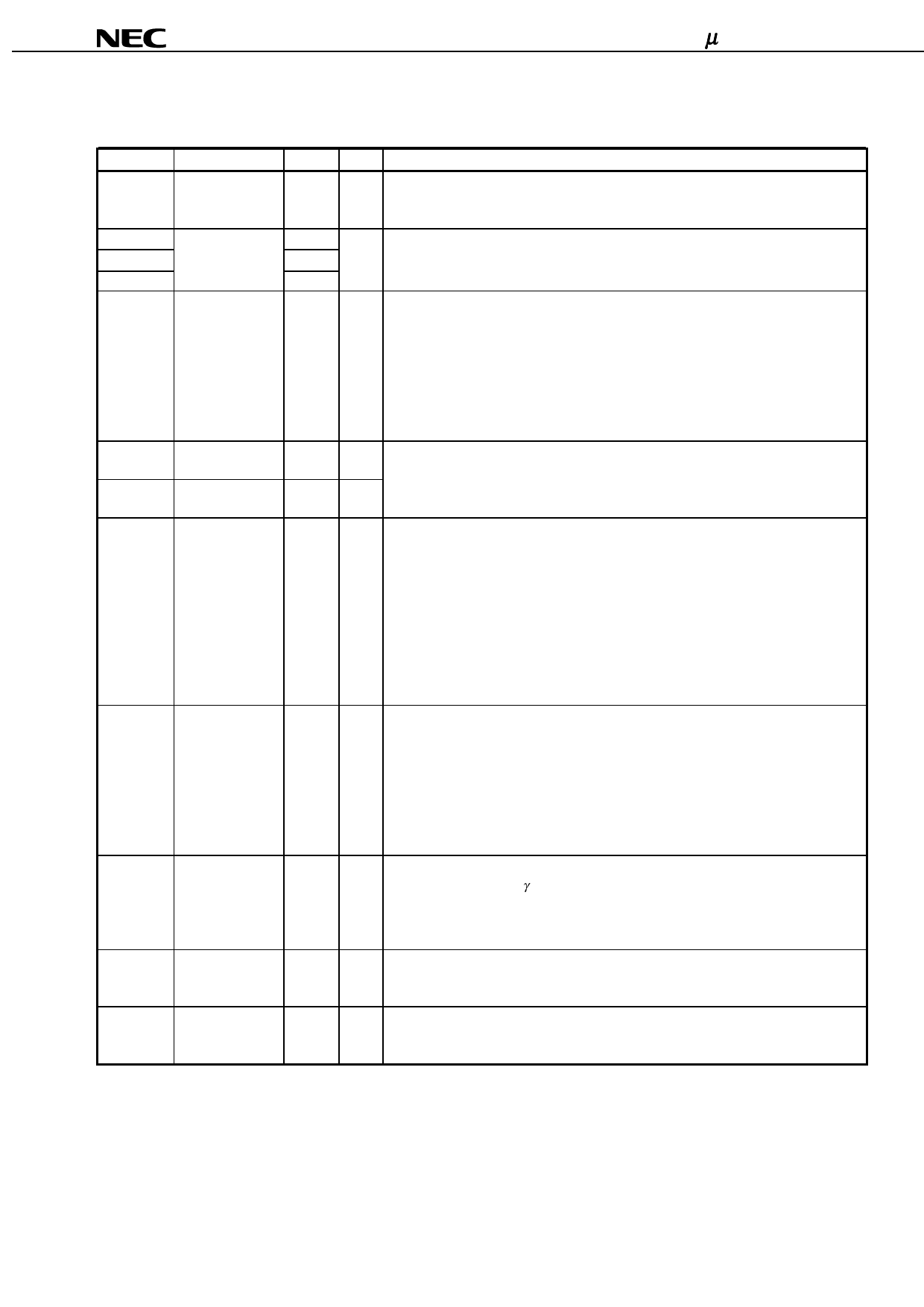
# 3. PIN FUNCTIONS
(1/2)
Pin Symbol
Pin Name
Pad No. I/O
Description
S1 to S396
D00 to D05
D10 to D15
D20 to D25
R,/L
STHR
STHL
CLK
STB
Driver output
Display data input
Shift direction
control input
Right shift start
pulse input/output
Left shift start
pulse input/output
Shift clock input
Latch input
1 to 396 Output The D/A converted 64-gray-scale analog voltage is output.
Osel = L: S1 to S396
Osel = H: S19 to S378
477 to 472
471 to 466
442 to 437
Input
The display data is input with a width of 18 bits, viz., the gray scale data (6 bits) by 3
dots (1 pixels).
DX0: LSB, DX5: MSB
429
Input These refer to the shift direction control input.
The shift directions of the shift registers are as follows.
<When in Osel = L>
R,/L = L (left shift): STHL (input), S396 → S1 → STHR (output)
R,/L = H (right shift) : STHR (input), S1 → S396 → STHL (output)
<When in Osel = H>
R,/L = L (left shift): STHL (input), S378 → S19 → STHR (output)
R,/L = H (right shift) : STHR (input), S19 → S378 → STHL (output)
498
I/O These refer to the start pulse I/O pins when driver ICs are connected in cascade.
Fetching of display data starts when H is read at the rising edge of CLK.
410
I/O R,/L = H (right shift): STHR input, STHL output
R,/L = L (left shift): STHL input, STHR output
443
Input This pin is the shift clock input of the shift register.
Display data is captured into the data register at the rising edge.
Osel = L: The start pulse output enters high level at the rising edge of the 132 th clock
following the start pulse input, and becomes the start pulse of the next level
driver. The 133th clock of the first driver becomes the start pulse input of the
next driver
Osel = H: The start pulse output enters high level at the rising edge of the 120th clock
following the start pulse input, and becomes the start pulse of the next driver.
The 121th clock of the first driver becomes the start pulse input of the next
driver.
436
Input A timing signal that latches the contents of the data register. When an H level is read
at the rising edge of CLK, the contents of the data register are latched and transferred
to the D/A converter, and analog voltage corresponding to the display data is output.
Also, because the internal operation via CLK continues even after the STB latch, do
not stop CLK. The contents of the shift register are cleared at the rising edge of STB.
Following a 1-pulse input at startup, this IC will operate normally. Note that the output
switch is turned off at the rising edge of STB.
For the STB input timing, refer to Switching Characteristics Waveform.
POL
Polarity inversion 434
signal
Input
This pin inverts the output polarity. The polarity inversion signal data is captured at the
rising edge of STB. The γ -resistor is switched in accordance with the positive/negative
polarity.
POL = L: Negative polarity
POL = H: Positive polarity
INV
VCOM
Data inversion 465
COM amplitude 409
output
Input This pin inverts the input data. Input data in synchronization with the shift clock.
INV = L: Normal input
INV = H: Data inversion input
Output This pin inverts the signal input from the POL pin and outputs it following conversion to
the VDD2 potential at the rising edge of STB. When the VCOM output is not used, VCsel
must be fixed to L.
Data Sheet S15381EJ1V0DS
7
Share Link: