UPD161622P 데이터 시트보기 (PDF) - NEC => Renesas Technology
부품명
상세내역
제조사
UPD161622P Datasheet PDF : 103 Pages
| |||
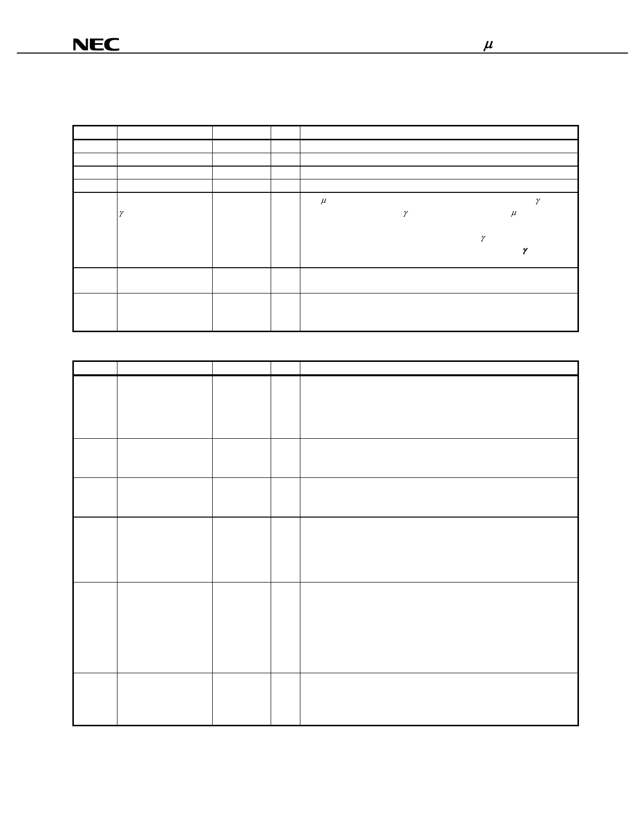
3. PIN FUNCTIONS
µ PD161622
3.1 Power Supply System Pins
Symbol
Pin Name
Pad No.
I/O
Function
VCC1
Logic power supply
71, 83, 84
− Power supply pin for logic circuit
VCC2
I/O power supply
57, 70
− Power supply pin for I/O buffer
VS
Driver power supply
78, 79
− Power supply pin for driver circuit
VSS
Ground
69, 72, 72, 80 − Ground pin for logic and driver circuits
V0 to V5 Power supply for
VRH
γ-curve correction
95 to 100,
94,
− The µ PD161622 includes power supplies and resistors for the γ-curve, so
if the characteristics of the γ-curve and LCD panel in the µ PD161622
VRL1, VRL2
101, 102
match, leave V0 to V5, VRH, VRL1, VRL2 open.
If some kind of correction is required, adjust the γ-curve by connecting
resistors between the V0 to V5, VRH, VRL1, VRL2 pins (see 5.9 γ-Curve
Correction Power Supply Circuit for Cases of Unbalanced Driving).
VCC1(MODE) Mode setting pull-up
27, 91, 124,
− Pull-up power-supply pin for mode setting
power-supply
128, 132
VSS(MODE) Mode setting pull-down 20, 29, 31, 33, 51, − Pull-down power-supply pin for mode setting
power-supply
60, 88, 93, 103,
115, 126, 130
3.2 Logic System Pins
Symbol
Pin Name
Pad No.
PSX
CPU interface selection 58
/CS
Chip select
52
/RESET Reset
53
/RD
Read
56
(E)
(enable)
/WR
Write
55
(R, /W) (read/write)
C86
Select interface
59
(1/2)
I/O
Function
Input These pins are used to select the CPU interface mode.
PSX = H: Parallel interface
PSX = L: Serial interface
When the parallel interface is selected, this data but width can be changed
between 8 bits and 16 bits by using BMD of index register 5 (R5).
Input This pin is used for chip select signals. When /CS = L, the chip is active
and can perform data input/output operations including command and data
I/O.
Input When /RESET is low, an internal reset is performed. The reset operation
is executed at the /RESET signal level. Be sure to perform reset via this
pin at power application.
Input When i80 series parallel data transfer (/RD) has been selected, the signal
at this pin is used to enable read operations. Data is output to the data bus
only when this pin is low.
When M68 series parallel data transfer (E) has been selected, the signal at
this pin is used to enable read/write operations.
Input When i80 series parallel data transfer (/WR) has been selected, the signal
at this pin is used to enable write operations. Data is written at the rising
edge of this signal.
When M68 series parallel data transfer (R, /W) and serial data has been
selected, this pin is used to determine the direction of data transfer.
L: Write
H: Read
Input This pin is used to switch between interface modes (i80 series CPU or M68
series CPU).
L: Selects i80 series CPU mode
H: Selects M68 series CPU mode
8
Data Sheet S15649EJ2V0DS
Share Link: 