UPD161831 데이터 시트보기 (PDF) - NEC => Renesas Technology
부품명
상세내역
제조사
UPD161831
NEC => Renesas Technology

UPD161831 Datasheet PDF : 67 Pages
| |||
µPD161831
3.4 Power Supply Function Control Pin
Pin Symbol
Pin Name
Pin Name I/O
Description
5 C1+/−,C2+/−, Booster capacitor 359 to 404
−
Connect the boost capacitor of the DC/DC converter to this pin.
C3+/−,C4+/−, connection
Booster ratio is difference on the way of using condenser connection.
C5+/−
For details, refer to figure 3−3.
VDC2
DC/DC converter 352 to 358
−
DC/DC converter boost output (VDC x 2 or VDC x 3). This output is the VS and
output
VR amplifier power supply. The VDC2 boot step is selected with the VCD2 bit.
VCD2 bit = 0: VDC x 2
VCD2 bit = 1: VDC x 3
VS
Source power
336 to 332
−
Source voltage output pin.
supply output
The VS output voltage can be changed through the VSEL0 to VSEL2.
MVS
External
417, 418
Input An external resistance can be input to set any output voltage.
resistance input
EXRV bit = 0: Leave open (Internal resistor selection)
EXRV bit = 1: Connect external resistor.
VR
Reference power 341 to 344
−
Gate reference power supply output pin.
supply output
The VR output voltage can be changed through the VRSEL to VRSEL2 setting.
VDD2
DC/DC converter 303 to 306,
−
DC/DC converter boost output (VGD x 2)
output
406, 407
VSS1
DC/DC converter 299 to 302,
−
DC/DC converter boost output (VGD x −1)
output
408 to 411
VSS2
DC/DC converter 295 to 298
−
DC/DC converter boost output (VGD x −2)
output
VDC
Reference power 345 to 351
−
Extension pin used to control circuit on panel.
supply input for
source power
supply voltage
VGD
Reference power 337 to 340
−
Extension pin used to control circuit on panel.
supply input for
gate power
supply voltage
DCCLK
Boost clock
405
input
Input Pin used to input boost clock of DC/DC converter.
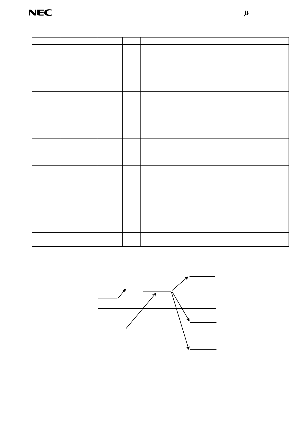
Figure 3−2. DC/DC Converter Boost Configuration
VCC: 2.5 to 3.6 V
VDC: 2.5 to 3.6 V
VSS: 0 V
VDC2: VDC x 2 or VDC x 3
VR, VS
VDD2: VR x 2 or VS x 2
Regulator outputs VR and VS are generated from VDC2.
The following voltages can be selected for VS and VR.
3.0 V, 3.5 V, 4.0 V, 4.5 V, 4.75 V, 5.0 V, 5.25 V, 5.5 V
VSS1: VR x −1 or VS x −1
VSS2: VR x −2 or VS x −2
Preliminary Product Information S16269EJ2V0PM
9
Share Link: