US2076CM 데이터 시트보기 (PDF) - Unisem
부품명
상세내역
제조사
US2076CM Datasheet PDF : 4 Pages
| |||
US2076
ABSOLUTE MAXIMUM RATINGS
12V Supply Voltage ............................................................. 14V
Vin Supply Voltage .............................................................. 7V
LDO Power Dissipation .................................... Internally Limited
FB Pin Voltage........................................................ -0.3V to 5V
Storage Temperature Range ................................. -65 TO 150°C
Operating Junction Temperature ............................... 0 TO 150°C
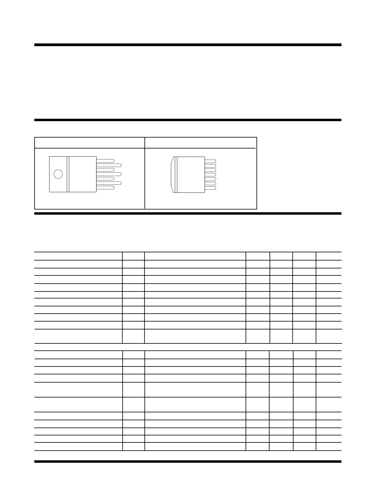
PACKAGE INFORMATION
7 PIN PLASTIC TO220 (T)
FRONT VIEW
7
6
5
4
3
2
1
Vin
Vout
Vfb2
Gnd
Vfb1
V12
Drv
θJT=2.7°C/W θJA=60°C/W
7 PIN PLASTIC TO263 (M)
FRONT VIEW
7
6
5
4
3
2
1
Vin
Vout
Vfb2
Gnd
Vfb1
V12
Drv
θJA=35°C/W for 1" Square pad
ELECTRICAL SPECIFICATIONS
Unless otherwise specified the following specification applies over,Vin=5V,V12=12V,and Tj=0 to 125°C.Low duty
cycle pulse testing are used which keeps junction and case temperatures equal to the ambient temperature.
LDO Section
PARAMETER
SYM
F.B Voltage Initial Accuracy Vfb2
F.B Voltage Total Variation
Vfb2
F.B Input Bias Current
Ifb2
Dropout Voltage (note 2)
Line Regulation
Load Regulation (note 1)
Thermal Regulation
Minimum Load Current (note 3)
Ripple Rejection
V12 Supply Current
Icc2
TEST CONDITION
Tj=25°C
Vfb2=1.25V
Vout=1.25V, Io=7.5A
Vout=1.25V,Io=10mA, 3<Vin<6V
Vout=1.25V, 10mA<Io<7.5A
30 mS Pulse
f=120HZ ,Co=25uF Tan,Io=1A
Vfb2=1V, Vfb1=1.5V, Io=7.5A
MIN
1.237
1.225
-1
TYP
1.250
1.250
1.1
0.2
0.5
0.01
70
75
MAX
1.262
1.275
+1
10
UNITS
V
V
uA
V
%
%
%/W
mA
dB
mA
Switching Controller Section
PARAMETER
SYM TEST CONDITION
F.B Voltage Initial Accuracy
Vfb1 Tj=25°C
F.B Voltage Total Variation
Vfb1
F.B Input Bias Current
Ifb1 Vfb1=1.25V
Min On Time
Vfb1 is sq wave with 300 ns on
time and 2 uS off time
Min Off Time
Vfb1 is sq wave with 300 ns off
time and 2 uS on time
V12 Supply Current
Icc1 Vfb1=1V, Vfb2=1.5V
Maximum Duty Cycle
Dmax Vfb1=1V
Minimum Duty Cycle
Dmin Vfb1=1.5V
Gate Drive Rise/Fall Time
Vgate Load=IRL3303
F.B Hysterises
MIN
1.237
1.225
-1
TYP
1.250
1.250
800
MAX
1.262
1.275
+1
UNITS
V
V
uA
nS
800
nS
10
mA
100
%
0
%
70
nS
12
mV
4-2
Rev. 1.3
4/26/98
Share Link: 