VRE3050 데이터 시트보기 (PDF) - Cirrus Logic
부품명
상세내역
제조사
VRE3050 Datasheet PDF : 6 Pages
| |||
®
Product Innovation From
VRE3050
3. THEORY OF OPERATION
The following discussion refers to the block diagram in Figure 1. A FET current source is used to bias a 6.3 V zener
diode. The zener voltage is divided by the resistor network R1 and R2. This voltage is then applied to the noninvert-
ing input of the operational amplifier which amplifies the voltage to produce a 5 V output. The gain is determined by
the resistor networks R3 and R4: G=1 + R4/R3. The 6.3 V zener diode is used because it is the most stable diode
over time and temperature.
The current source provides a closely regulated zener current, which determines the slope of the references’ volt-
age vs. temperature function. By trimming the zener current a lower drift over temperature can be achieved. But
since the voltage vs. temperature function is nonlinear this compensation technique is not well suited for wide tem-
perature ranges.
A nonlinear compensation network of thermistors and resistors that is used in the VRE series voltage references.
This proprietary network eliminates most of the nonlinearity in the voltage vs. temperature function. By adjusting the
slope, a very stable voltage is produced over wide temperature ranges.
This network is less than 2% of the overall network resistance so it has a negligible effect on long term stability. The
proper connection of the VRE3050 series voltage references with the optional trim resistor for initial error and the
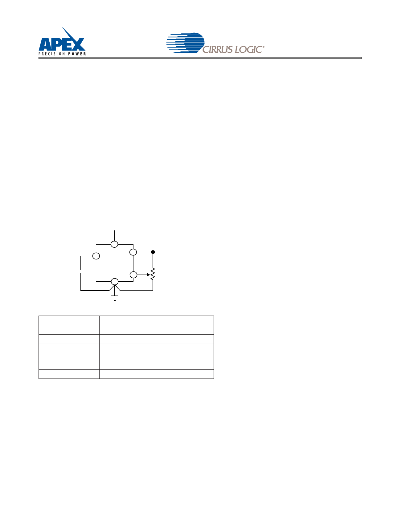
optional capacitor for noise reduction is shown below.
EXTERNAL CONNECTIONS
+ VIN
Optional Noise
Reduction
Capacitor
CN 1µF
2
8
6
VRE3050
5
4
+ VOUT
10kΩ
Optional Fine
Trim Adjustment
PIN DESCRIPTION
1, 3, 7 N. C. Internally connected. Do not use
2
VIN
Positive power supply input
4
GND Ground
5
TRIM External trim input. Leave open if not
used.
6
OUT
Voltage reference output
8
NR
Noise Reduction
4. BASIC CIRCUIT CONNECTION
To achieve the specified performance, pay careful attention to the layout. A low resistance star configuration will
reduce voltage errors, noise pickup, and noise coupled from the power supply. Commons should be connected to
a single point to minimize interconnect resistances.
VRE3050DS
5
Share Link: 