VRE410A 데이터 시트보기 (PDF) - Cirrus Logic
부품명
상세내역
제조사
VRE410A Datasheet PDF : 5 Pages
| |||
VRE410
Product Innova tionFrom
3. THEORY OF OPERATION
The following discussion refers to the block diagram in Figure 1. In operation, approximately 6.3 V is applied to
the noninverting input of the op amp. The voltage is amplified by the op amp to produce a 10 V output. The gain is
determined by the networks R1 and R2: G=1 + R2/R1. The 6.3 V zener diode is used because it is the most stable
diode over time and temperature.
The zener operating current is derived from the regulated output voltage through R3. This feedback arrangement
provides a closely regulated zener current. This current determines the slope of the references’ voltage vs. tempera-
ture function. By trimming the zener current a lower drift over temperature can be achieved. But since the voltage
vs. temperature function is nonlinear this compensation technique is not well suited for wide temperature ranges.
A nonlinear compensation network of thermistors and resistors is used in the VRE series voltage references. This
proprietary network eliminates most of the nonlinearity in the voltage vs. temperature function. By then adjusting the
slope, a very stable voltage is produced over wide temperature ranges.
The VRE400 series voltage references have the ground terminal brought out on two pins (pin 6 and 7) which are
connected together internally. This allows the user to achieve greater accuracy when using a socket. Voltage ref-
erences have a voltage drop across their power supply ground pin due to quiescent current flowing through the
contact resistance. If the contact resistance was constant with time and temperature, this voltage drop could be
trimmed out. When the reference is plugged into a socket, this source of error can be as high as 20 ppm. By con-
necting pin 7 to the power supply ground and pin 6 to a high impedance ground point in the measurement circuit,
the error due to the contact resistance can be eliminated. If the unit is soldered into place the contact resistance is
sufficiently small that it doesn’t effect performance.
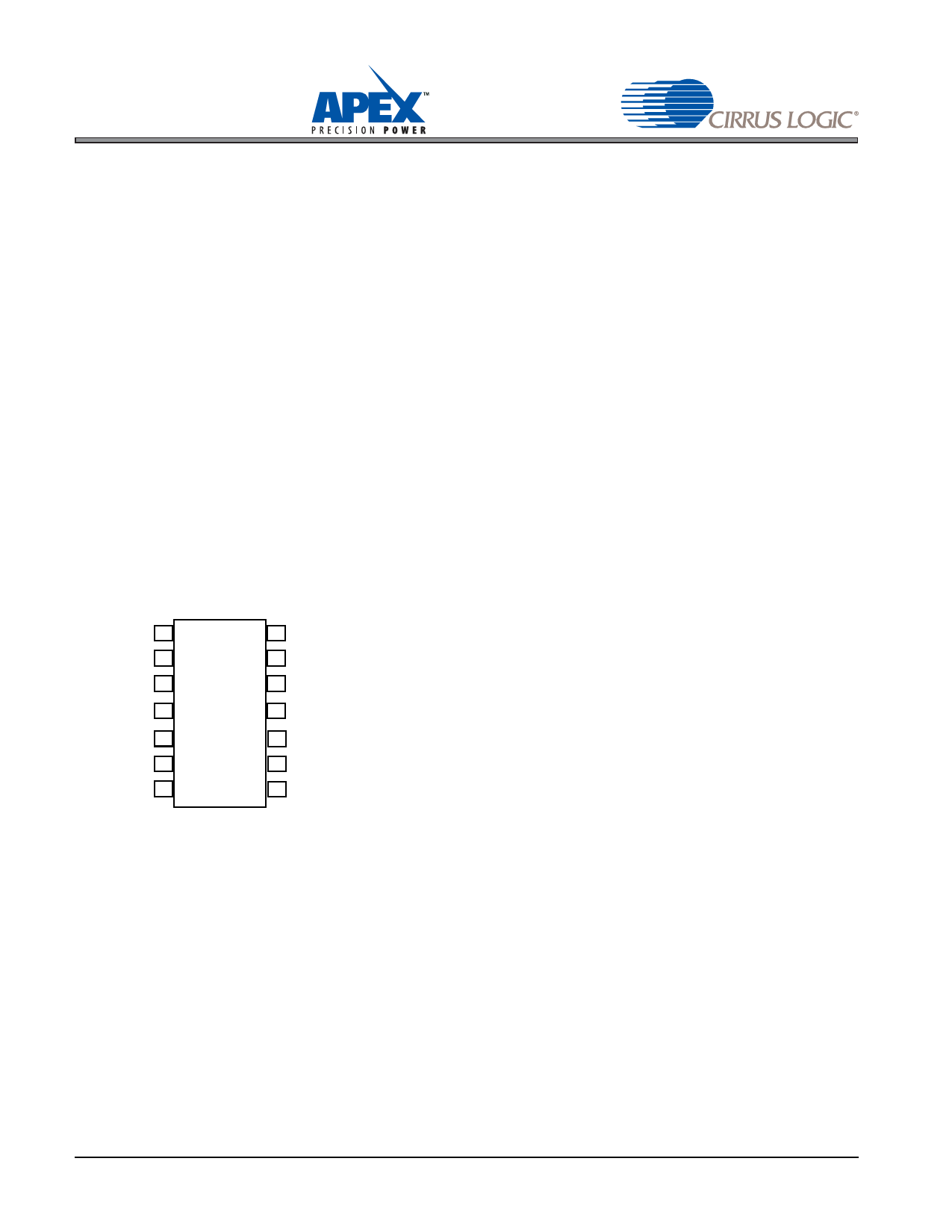
PIN CONFIGURATION
N/C 1
- VOUT 2
N/C 3
- VIN 4
N/C 5
REF. GND 6
GND 7
VRE410
TOP
VIEW
14 N/C
13 +VOUT
12 N/C
11 +VIN
10 N/C
9 N/C
8 N/C
VRE410DS
Share Link: 