WED3C7410E16M-400BX 데이터 시트보기 (PDF) - White Electronic Designs Corporation
부품명
상세내역
제조사
WED3C7410E16M-400BX Datasheet PDF : 13 Pages
| |||
White Electronic Designs WED3C7410E16M-400BX
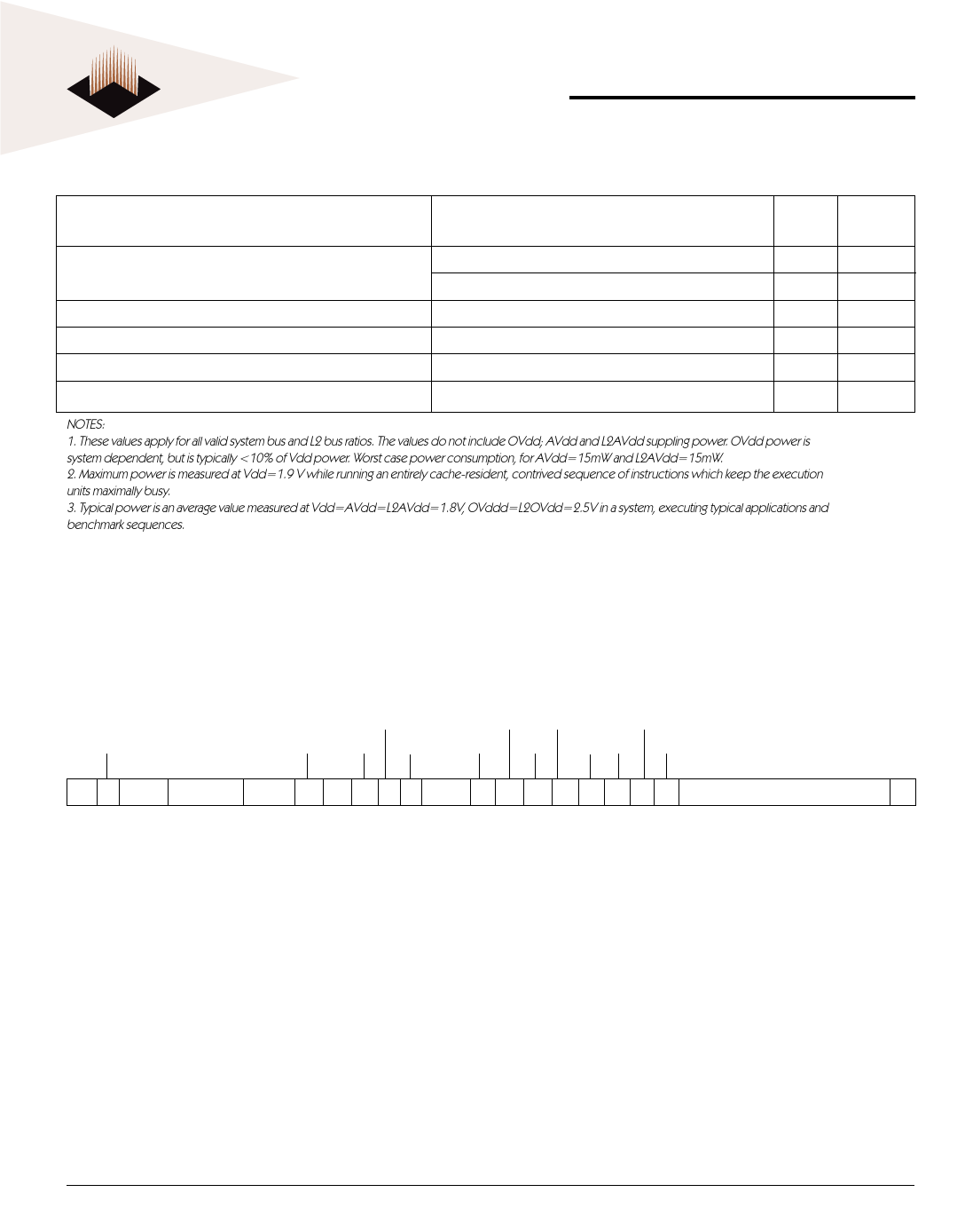
POWER CONSUMPTION
VDD=AVDD=1.8±0.1V VDC, L2VDD=3.3V ±5% VDC, GND=0 VDC, 0≤TJ<105°C
Full-on Mode
Doze Mode
Nap Mode
Sleep Mode
Sleep Mode–PLL and DLL Disabled
Processor (CPU) Frequency/L2 Frequency
400 MHz/200MHz
Unit Notes
Typical
5.7
W
1, 3
Maximum
13.5
W
1, 2
Maximum
5.3
W
1, 2
Maximum
2.25
W
1, 2
Maximum
2.20
W
1, 2
Maximum
2.0
W
1, 2
NOTES:
1. These values apply for all valid system bus and L2 bus ratios. The values do not include OVdd; AVdd and L2AVdd suppling power. OVdd power is
system dependent, but is typically <10% of Vdd power. Worst case power consumption, for AVdd=15mW and L2AVdd=15mW.
2. Maximum power is measured at Vdd=1.9 V while running an entirely cache-resident, contrived sequence of instructions which keep the execution
units maximally busy.
3. Typical power is an average value measured at Vdd=AVdd=L2AVdd=1.8V, OVddd=L2OVdd=2.5V in a system, executing typical applications and
benchmark sequences.
L2 CACHE CONTROL REGISTER (L2CR)
The L2 cache control register, shown in Figure 5, is a supervisor-level, implementation-specific SPR used to configure and
operate the L2 cache. It is cleared by hard reset or power-on reset.
FIG. 5 L2 CACHE CONTROL REGISTER (L2CR)
L2PE
L2IP
L2E L2SIZ
L2CLK
L2WT
L2DO L2CTL L2TS
L2DF L2FA L2CLKSTP
L2SL L2BYP L2HWF L2IO L2DRO
L2RAM L21
L2OH
0000000
01 2 3 4
6 7 8 9 10 11 12 13 14 15 16 17 18 19 20 21 22 23 24
The L2CR bits are described in Table 1.
30 31
White Electronic Designs Corporation • Phoenix AZ • (602) 437-1520
8
Share Link: 