WED3C7410E16M400BC 데이터 시트보기 (PDF) - White Electronic Designs Corporation
부품명
상세내역
제조사
WED3C7410E16M400BC Datasheet PDF : 13 Pages
| |||
White Electronic Designs WED3C7410E16M-XBX
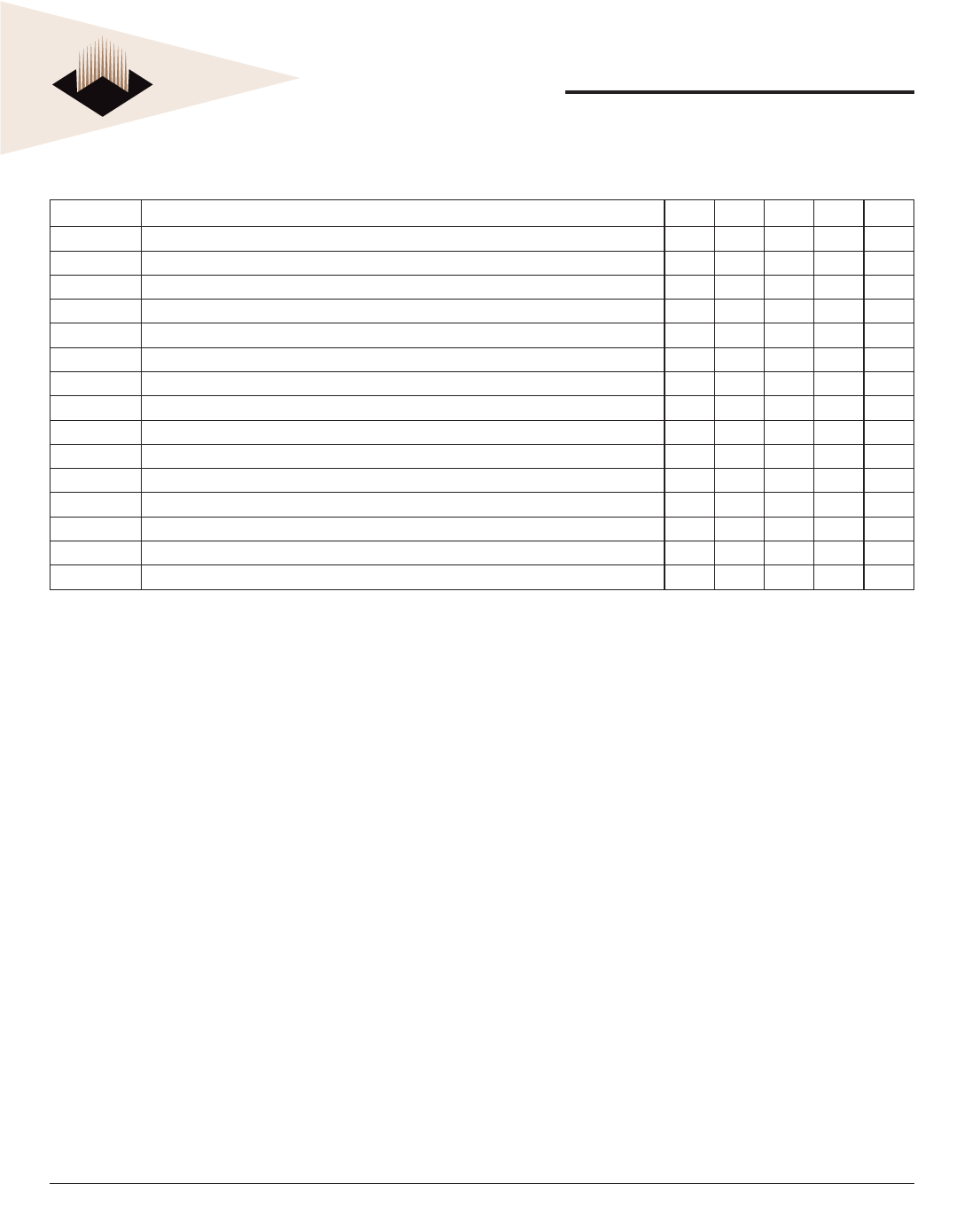
PACKAGE PINOUT LISTING (continued)
Signal Name
SYSCLK
TA#
TBEN
TBST#
TCK
TDI (6)
TDO
TEA#
TMS (6)
TRST# (6)
TS#
TSIZ[0-2]
TT[0-4]
VCC (2)
WT#
Pin Number
C9
H14
C2
A14
C11
A11
A12
H13
B11
C10
J13
A13, D10, B12
B13, A15, B16, C14, C15
F6, F8, F9, F11, G7, G10, H4, H6, H8, H9, H11, J6, J8, J9, J11, K7, K10, L6, L8, L9
D2
Active
—
Low
High
Low
High
High
High
Low
High
Low
Low
High
High
—
Low
I/O 1.8V (7) 2.5V (7) 3.3V (7)
Input
Input
Input
Output
Input
Input
Output
Input
Input
Input
I/O
Output
I/O
Input 1.8V 1.8V 1.8V
I/O
NOTES:
1. These are test signals for factory use only and must be pulled up to OVCC for
normal machine operation.
2. OVCC inputs supply power to the I/O drivers and VCC inputs supply power to the
processor core.
3. To allow future L2 cache I/O interface voltage changes.
4. To allow processor bus I/O voltage changes, provide the option to connect BVSEL
to HRESET# (Selects 2.5V Interface) or to GND (Selects 1.8V Interface) or to
OVCC (Selects 3.3V Interface).
5. Uses one of 9 existing no-connects in WEDC’s WED3C755A8M-XBX.
6. Internal pull up on die.
7. OVCC supplies power to the processor bus, JTAG, and all control signals except
the L2 cache controls (L2CE, L2WE, and L2ZZ); L2OVCC supplies power to the L2
cache I/O interface (L2ADDR (0-18], L2DATA (0-63), L2DP{0-7] and L2SYNC-
OUT) and the L2 control signals; L2AVCC supplies power to the SSRAM core
memory; and VCC supplies power to the processor core and the PLL and DLL (after
filtering to become AVCC and L2AVCC respectively). These columns serve as a
reference for the nominal voltage supported on a given signal as selected by the
BVSEL pin configuration and the voltage supplied. For actual recommended value
of Vin or supply voltages see Recommended Operating Conditions.
8. Output only for 7410, was I/O for 750/755.
9. Enhanced mode only.
10. Deasserted (pulled high) at HRESET# for 60x bus mode.
11. Reuses 750/755 DRTRY#, DBIS#, and TLBISYNC pins (DTI1, DTI2, and EMODE#
respectively).
12. Unused output in 60x bus mode.
13. Connect to HRESET# to trigger post power-on-reset (por) internal memory test.
14. Ignored in 60x bus mode.
May 2006
Rev. 9
6
White Electronic Designs Corporation • (602) 437-1520 • www.wedc.com
Share Link: 