WED3C7410E16M400BC 데이터 시트보기 (PDF) - White Electronic Designs Corporation
부품명
상세내역
제조사
WED3C7410E16M400BC Datasheet PDF : 13 Pages
| |||
White Electronic Designs WED3C7410E16M-XBX
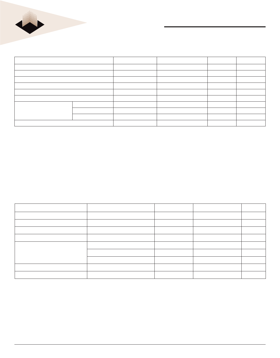
ABSOLUTE MAXIMUM RATINGS
Characteristic
Symbol
Value
Unit
Notes
Core supply voltage
PLL supply voltage
L2 DLL supply voltage
60x bus supply voltage
L2 bus supply voltage
L2 supply voltage
Input supply
Storage temperature range
Processor Bus
L2 bus
JTAG Signals
VCC
AVCC
L2AVCC
OVCC
L2OVCC
L2VCC
VIN
VIN
VIN
TSTG
-0.3 to 2.1
-0.3 to 2.1
-0.3 to 2.1
-0.3 to 3.465
-0.3 to 2.6
-0.3 to 4.6
-0.3 to 0VCC +0.2
-0.3 to L20VCC +0.2
-0.3 to OVCC +0.2
-55 to 150
V
(4)
V
(4)
V
(4)
V
(3)
V
(3)
V
(5)
V
(2)
V
(2)
V
(2)
°C
NOTES:
1. Functional and tested operating conditions are given in Operating Conditions table. Absolute maximum ratings are stress ratings only, and functional operation at the maximums is
not guaranteed. Stresses beyond those listed may affect device reliability or cause permanent damage to the device.
2. Caution: Vin must not exceed OVCC by more than 0.2V at any time including during power-on reset.
3. Caution: OVCC/L2OVCC must not exceed VCC/AVCC/L2AVCC by more than 2.0 V at any time including during power-on reset.
4. Caution: VCC/AVCC/L2AVCC must not exceed L2OVCC/OVCC by more than 0.4 V at any time including during power-on reset.
5. L2OVCC should never exceed L2VCC
RECOMMENDED OPERATING CONDITIONS
CHARACTERISTIC
SYMBOL
RECOMMENDED VALUE
Core supply voltage
VCC
1.8v ± 100mV
PLL supply voltage
AVCC
1.8v ± 100mV
L2 DLL supply voltage
L2AVCC
1.8v ± 100mV
Memory core supply voltage
L2VCC
3.3v ± 165mV
BVSEL = 0
OVCC
1.8± 100mV
Processor bus supply voltage
BVSEL = HRESET#
OVCC
2.5v ± 100mV
BVSEL = HRESET or BVSEL = 1
OVCC
3.3v ± 165 mV
L2 bus supply voltage
L2VSEL = HRESET# or 1
L20VCC
2.5v ± 100 mV
Input Voltage
Processor bus and JTAG Signals
Vin
GND to OVCC
NOTE: These are the recommended and tested operating conditions. Proper device operation outside of these conditions is not guaranteed
UNIT
V
V
V
V
V
V
V
V
V
May 2006
Rev. 9
7
White Electronic Designs Corporation • (602) 437-1520 • www.wedc.com
Share Link: 