ICX062AL 데이터 시트보기 (PDF) - Sony Semiconductor
부품명
상세내역
제조사
ICX062AL Datasheet PDF : 16 Pages
| |||
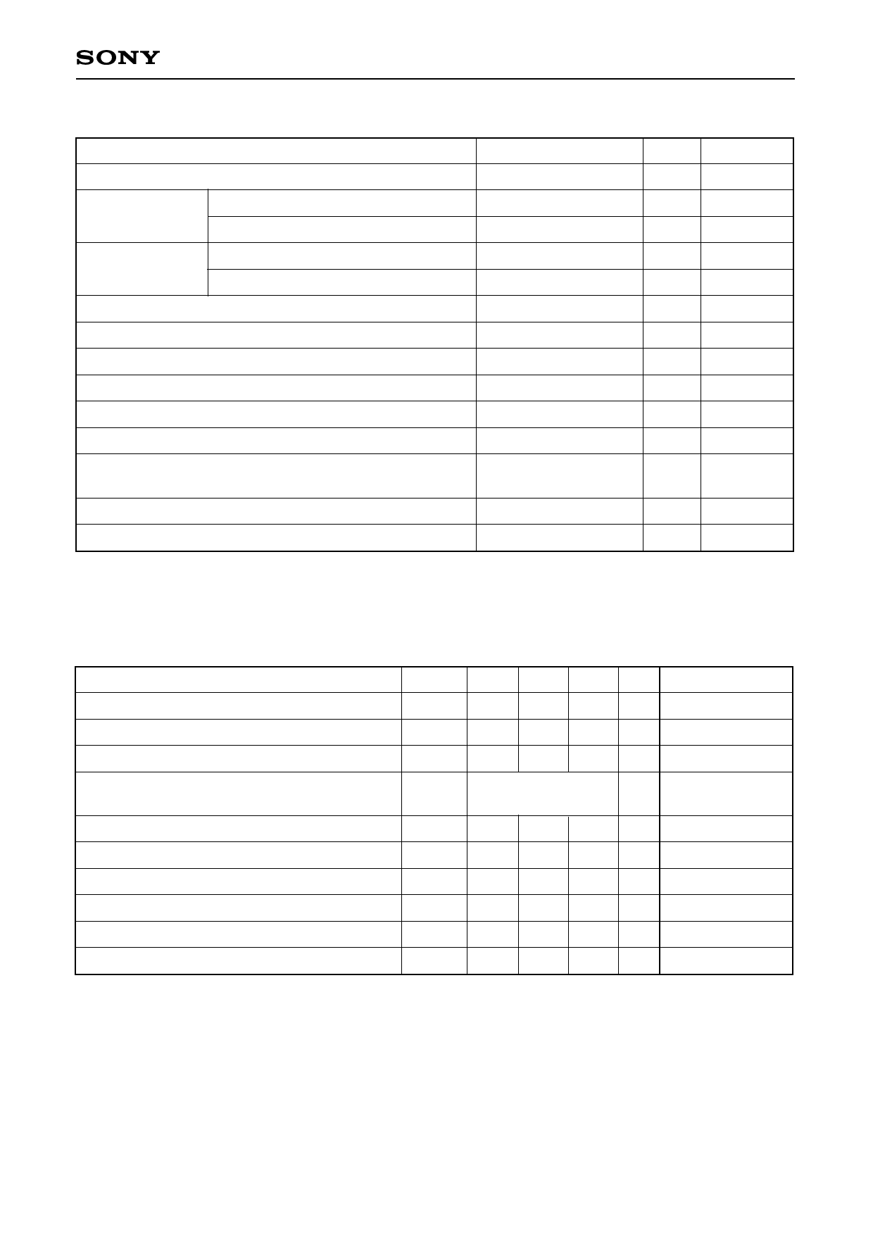
Absolute Maximum Ratings
Item
Substrate voltage SUB – GND
Supply voltage
HIS, VDD, RD, VOUT, VSS – GND
HIS, VDD, RD, VOUT, VSS – SUB
Vertical, horizontal Vφ1, Vφ2, Vφ3, Vφ4, Hφ1, Hφ2 – GND
clock input voltage Vφ1, Vφ2, Vφ3, Vφ4, Hφ1, Hφ2 – SUB
Ratings
–0.3 to +55
–0.3 to +20
–55 to +10
–15 to +20
–65 to +10
Voltage difference between vertical clock input pins
to +15
Voltage difference between horizontal clock input pins
Hφ1, Hφ2 – Vφ4
RG, VGG – GND
RG, VGG – SUB
to +17
–17 to +17
–10 to +15
–55 to +10
VL – SUB
Vφ1, Vφ2, Vφ3, Vφ4, Hφ1, Hφ2, HIS, VDD, RD, VOUT,
VSS, RG, VGG – VL
–65 to +0.3
–0.3 to +30
Storage temperature
–30 to +80
Operating temperature
–10 to +60
∗1 +27V (max.) when clock width < 10µs and the clock duty factor < 0.1%.
ICX062AL
Unit Remarks
V
V
V
V
V
V
∗1
V
V
V
V
V
V
°C
°C
Bias Conditions
Item
Output amplifier drain voltage
Reset drain voltage
Output amplifier gate voltage
Output amplifier source
Substrate voltage adjustment range
Substrate voltage adjustment accuracy
Reset gate clock voltage adjustment range
Reset gate clock voltage adjustment accuracy
Protective transistor bias
Horizontal register input source bias
Symbol Min. Typ. Max. Unit
Remarks
VDD
14.7 15.0 15.3 V
VRD
14.7 15.0 15.3 V VRD = VDD
VGG
1.6 2.0 2.6 V
VSS
VSUB
Grounded with
390Ω resistor
9
19
±5%
V ∗1
∆VSUB
–3
VRGL
0
+3 %
3.0 V ∗1
∆VRGL
–3
VL
–13
+3 %
–10 V ∗2
VHIS
14.7 15.0 15.3 V VHIS = VDD
–3–
Share Link: 