XD010-04S-D4F 데이터 시트보기 (PDF) - Sirenza Microdevices => RFMD
부품명
상세내역
제조사
XD010-04S-D4F Datasheet PDF : 5 Pages
| |||
XD010-04S-D4F 350-600 MHz 12W Power Amp Module
Quality Specifications
Parameter
ESD Rating
Human Body Model, JEDEC Document - JESD22-A114-B
MTTF
85oC Leadframe, 200oC Channel
Unit
V
Hours
Typical
8000
1.2 X 10⁶
Pin Description
Pin #
Function
1
RF Input
2
VD1
3
VD2
4
RF Output
Flange
Gnd
Description
Module RF input. This pin is internally connected to DC ground. Do not apply DC voltages to the RF leads. Care must be
taken to protect against video transients that may damage the active devices.
This is the drain voltage for the first stage. Nominally +28Vdc
This is the drain voltage for the 2nd stage of the amplifier module. The 2nd stage gate bias is temperature compensated to
maintain constant quiscent drain current over the operating temperature range. See Note 1.
Module RF output. This pin is internally connected to DC ground. Do not apply DC voltages to the RF leads. Care must be
taken to protect against video transients that may damage the active devices.
Exposed area on the bottom side of the package needs to be mechanically attached to the ground plane of the board for
optimum thermal and RF performance. See mounting instructions in application note AN-060 on Sirenza’s web site.
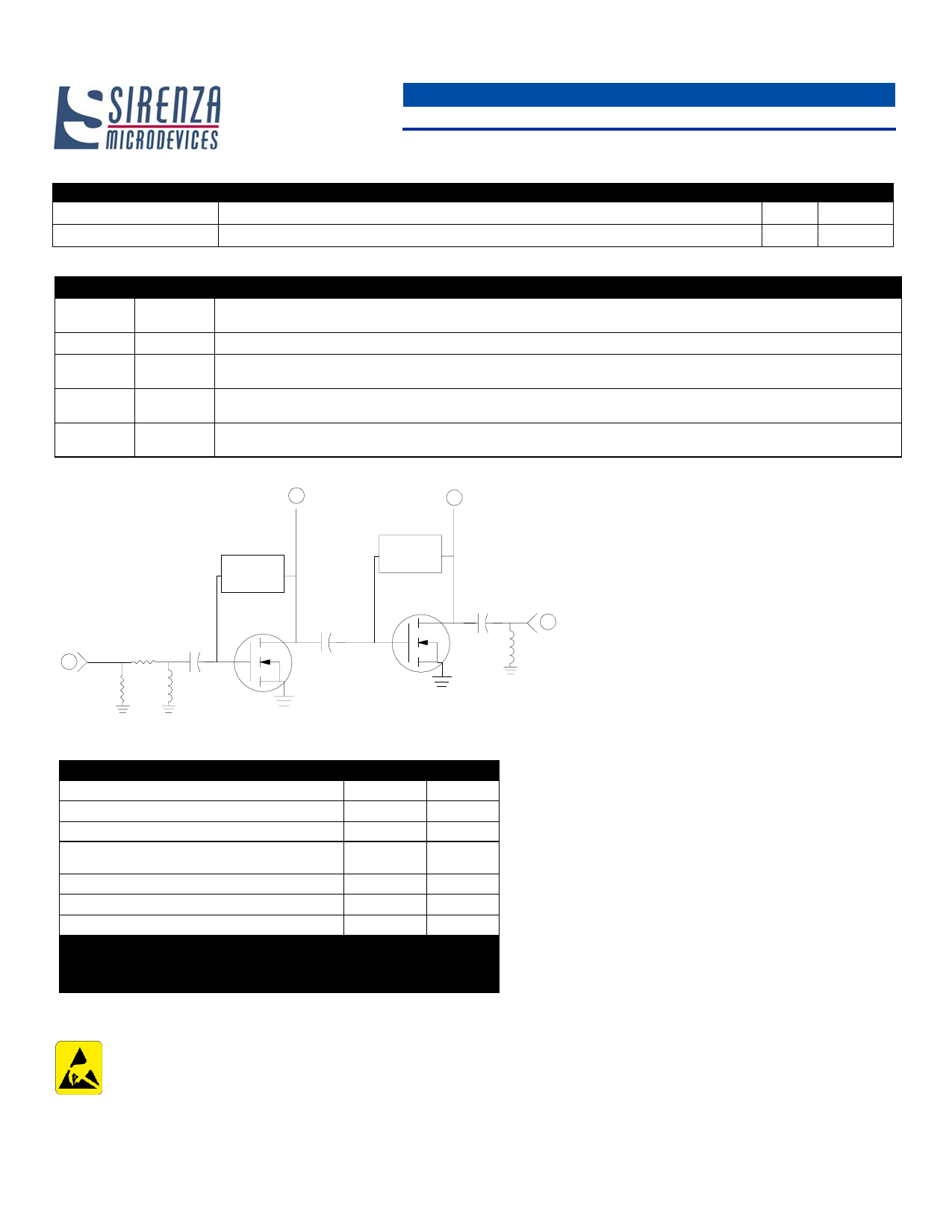
Simplified Device Schematic
2 VD1
3 VD2
RFin
1
Bias
Network
Q1
Temperature
Compensation
Q2
RFout
4
Case Flange = Ground
Absolute Maximum Ratings
Parameters
1st Stage Bias Voltage (VD1 )
2nd Stage Bias Voltage (VD2)
RF Input Power
Value
35
35
+20
Unit
V
V
dBm
Load Impedance for Continuous Operation With-
out Damage
5:1
VSWR
Output Device Channel Temperature
+200
ºC
Operating Temperature Range
-20 to +90
ºC
Storage Temperature Range
-40 to +100
ºC
Operation of this device beyond any one of these limits may cause per-
manent damage. For reliable continuous operation see typical setup val-
ues specified in the table on page one.
Caution: ESD Sensitive
Appropriate precaution in handling, packaging
and testing devices must be observed.
303 S. Technology Court
Broomfield, CO 80021
Phone: (800) SMI-MMIC
2
Note 1:
The internally generated gate voltage is thermally compen-
sated to maintain constant quiescent current over the temper-
ature range listed in the data sheet. No compensation is
provided for gain changes with temperature. This can only be
accomplished with AGC external to the module.
Note 2:
Internal RF decoupling is included on all bias leads. No addi-
tional bypass elements are required, however some applica-
tions may require energy storage on the drain leads to
accommodate time-varying waveforms.
Note 3:
This module was designed to have its leads hand soldered to
an adjacent PCB. The maximum soldering iron tip tempera-
ture should not exceed 700° F, and the soldering iron tip
should not be in direct contact with the lead for longer than 10
seconds. Refer to app note AN060 (www.sirenza.com) for fur-
ther installation instructions.
http://www.sirenza.com
EDS-104259 Rev E
Share Link: 