LT119AH 데이터 시트보기 (PDF) - Linear Technology
부품명
상세내역
제조사
LT119AH Datasheet PDF : 12 Pages
| |||
LT119A/LT319A
LM119/LM319
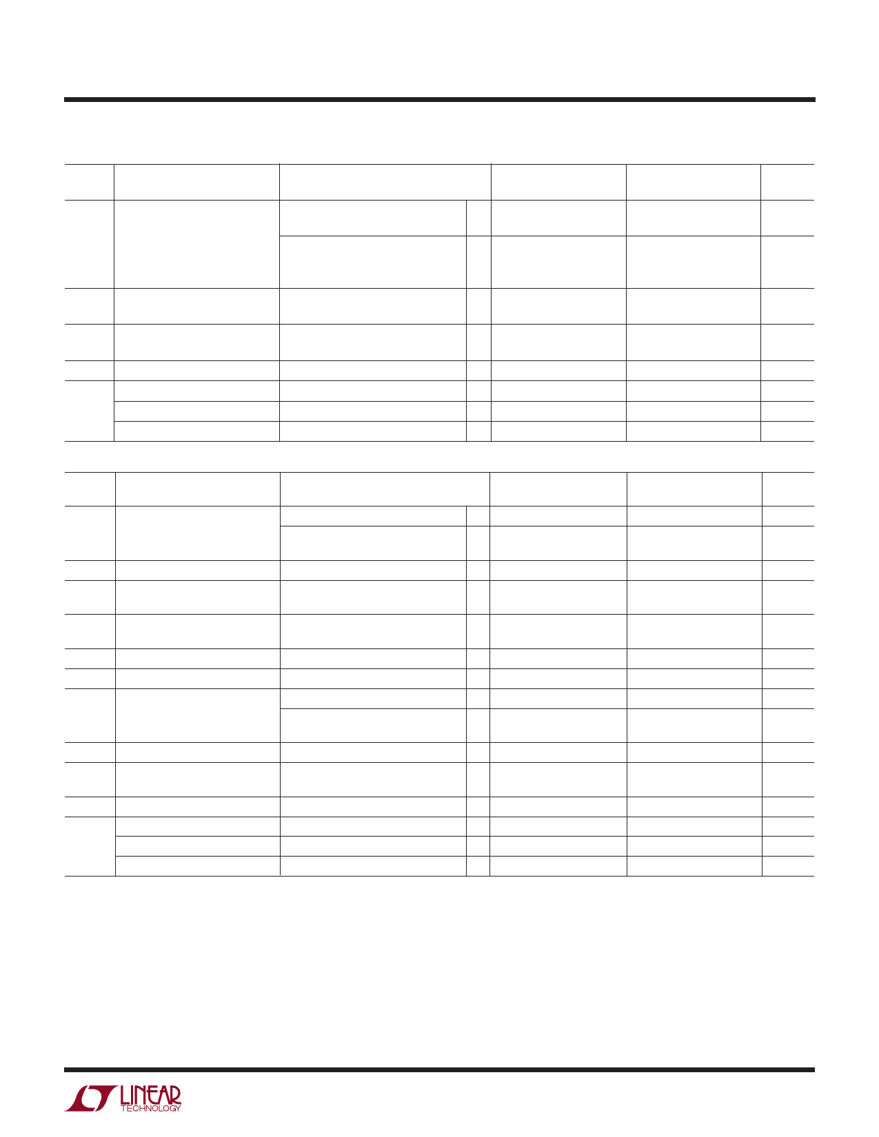
ELECTRICAL CHARACTERISTICS The q denotes the specifications which apply over the full operating
temperature range, otherwise specifications are at TA = 25°C. (Note 3)
SYMBOL PARAMETER
CONDITIONS
LT119A
MIN TYP MAX
LM119
MIN TYP MAX
UNITS
VSAT
Saturation Voltage
VIN ≤ –5mV, IO = 25mA,
V+ ≥ 4.5V, V– = 0V
0.75 1.5
0.75 1.5
V
Output Leakage Current
VIN ≤ –6mA, ISINK ≤ 3.2mA
TA ≥ 0°C
TA ≤ 0°C
VIN ≥ 5mV, VOUT to V– = 35V
q
0.23 0.4
0.6
0.2 2
1
10
0.23 0.4
V
0.6
V
0.2 2
µA
1
10
µA
Input Voltage Range
VS = ±15V
V+ = 5V, V– = 0V
q –12 ±13 12
–12 ±13 12
V
q1
3
1
3
V
Differential Input Voltage
IS
Supply Current
V+ = 5V, V– = 0V
Positive Supply Current
VS = ±15V
Negative Supply Current
VS = ±15V
q
±5
4.3
8 11.5
3 4.5
±5
V
4.3
mA
8 11.5
mA
3 4.5
mA
The q denotes the specifications which apply over the full operating temperature range, otherwise specifications are at TA = 25°C. (Note 3)
SYMBOL PARAMETER
CONDITIONS
LT319A
MIN TYP MAX
LM319
MIN TYP MAX
UNITS
VOS
Input Offset Voltage
VS = ±15V, VCM = 0V
RS ≤ 5k
(Note 4)
0.3 0.5
0.5 1
q
2
8
mV
2
8
mV
10
mV
CMRR Common Mode Rejection Ratio
90 106
dB
IOS
Input Offset Current
(Note 4)
30 40
q
60
80 200
nA
300
nA
IB
Input Bias Current
(Note 4)
150 500
q
1000
250 1000
nA
1200
nA
AV
Voltage Gain
Response Time
(Note 5)
20 40
80
8
40
80
V/mV
ns
VSAT
Saturation Voltage
VIN ≤ –10mV, ISINK = 25mA
0.75 1.5
0.75 1.5
V
V+ ≥ 4.5V, V– = 0V,
q
VIN ≤ –10mV, ISINK ≤ 3.2mA
0.3 0.4
0.3 0.4
V
Output Leakage Current
VIN ≥ 10mV, VOUT to V– = 35V
0.2 10
0.2 10
µA
Input Voltage Range
VS = ±15V
V+ = 5V, V– = 0V
q
±13
±13
V
q1
3
1
3
V
Differential Input Voltage
IS
Supply Current
V+ = 5V, V– = 0V
Positive Supply Current
VS = ±15V
Negative Supply Current
VS = ±15V
q
±5
4.3
8 12.5
3
5
±5
V
4.3
mA
8 12.5
mA
3
5
mA
Note 1: Absolute Maximum Ratings are those values beyond which the life
of a device may be impaired.
Note 2: For supply voltages less than ±15V, the maximum input voltage is
equal to the supply voltage.
Note 3: Unless otherwise noted, supply voltage equals ±15V and
VCM = 0V, TA = 25°C. The ground pin is grounded. Note that the maximum
voltage allowed between the ground pin and V+ is 18V. Do not tie the
ground pin to V– when the power supply voltage exceeds ±9V. The offset
voltage, offset current and bias current specifications apply for all supply
voltages between ±15V and 5V unless otherwise specified.
Note 4: The offset voltages and currents given are the maximum values
required to drive the output within 1V of either supply with a 1mA load,
thus these parameters define an error band and take into account the
worst case effects of voltage gain and input impedance.
Note 5: Response time specified is for a 100mV input step with 5mV
overdrive.
Note 6: Inputs are protected with back-to-back 5.6V zener diodes. This
limits maximum differential input voltage to ±5V if current is unlimited.
Larger differential input drive is allowed if input current is limited to ±5mA
with external resistance.
119a319afb
3
Share Link: 