MC13030 데이터 시트보기 (PDF) - Motorola => Freescale
부품명
상세내역
제조사
MC13030 Datasheet PDF : 16 Pages
| |||
MC13030
Therefore, its gain is determined by the load impedance
connected between Pins 15 and 16. Pin 16 is a voltage
reference for the output. The output is internally connected to
the AM detector, and Pin 13 is the detector output. This
detector also provides the AGC signal for the IF amplifier. An
RC filter from Pin 13 to 12 removes the audio, leaving a dc
level proportional to the carrier level for AGC.
Pin 11 provides a current proportional to signal strength.
It is a current source so a resistor must be connected from
Pin 11 to ground to select the desired dc voltage range. The
current is proportional to the signal level at Pin 17, the IF
amplifier input.
A high–gain limiting amplifier is used to derive the station
detect (SD) signal output on Pin 10; this output is present only if
it is turned on by the voltage on Pin 8. If the voltage on
Pin 8 is less than the voltage on Pin 11, the output on Pin 10 is
“on”. The station detector IF output on Pin 10 is used with
synthesizers which have a frequency counting signal detector.
The RF AGC outputs on Pins 4 and 5 are controlled by the
signal levels at Mixer1 or Mixer2. Bypass capacitors are
required on Pins 6 and 4 to remove audio signals from the
AGC outputs. Pin 4 is designed to control the NPN transistor
in series with the RF amplifier FET. The voltage on Pin 4 is
5.1 V with no input signal and decreases with increasing input
signal. Pin 5 is designed to control an additional AGC circuit
at the antenna input. The voltage on Pin 5 is at 0 V with no
input signal and increases with increasing input signals. The
voltage on Pin 5 does not increase until the voltage on Pin 4
has decreased to about 1.3 V. In most cases, Pin 5 is used to
drive a diode shunt. Maximum output current is about 850 µA.
The RF AGC sensitivity is about 40 mVrms input to Mixer1
or about 2.0 mVrms input to Mixer2 at 1.0 MHz. The AGC
sensitivity for both mixers can be decreased by adding a
resistor from Pin 6 to ground. There is also an additional
amplifier between Mixer1 and its AGC rectifier. The gain of
this amplifier and AGC sensitivity for Mixer1 can be increased
by adding a resistor from Pin 7 to ground. Therefore, the
desired AGC sensitivity for both mixers can be achieved by
changing the resistors on Pins 6 and 7.
Figure 2. Pin Connections and DC Voltages
3.3 V 1 Mix1 In
VCO Out 28 5.1 V
3.3 V 2 Mix1 In
VCO 27 5.1 V
0 V 3 RF Gnd
VCO Ref 26 5.1 V
5.1 to 0 V 4 FET RF AGC Mix1 Out 25 7.8 V
0 to 850 µA
0 to 2.8 V
5
RF AGC2
200 mV 6 RF AGC Adj
Mix1 Out 24 7.8 V
Vref 23 6.5 V
43 mV 7 Mix1 RF AGC Adj Mix2 In 22 3.7 V
0 to 4.8 V 8 SD Level
Mix2 Out 21 7.9 V
0 V 9 IF Gnd
Mix2 Out 20 7.9 V
6.5 V 10 SD IF Out
Xtal Osc E 19 4.4 V
0 to 4.8 V 11 S Level Out Xtal Osc B 18 5.0 V
3.6 to 4.5 V 12 IF AGC In
IF In 17 4.8 V
3.6 to 4.5 V 13 AF Out
8.0 V 14 VCC
Det Vref 16 4.1 V
Det In 15 4.1 V
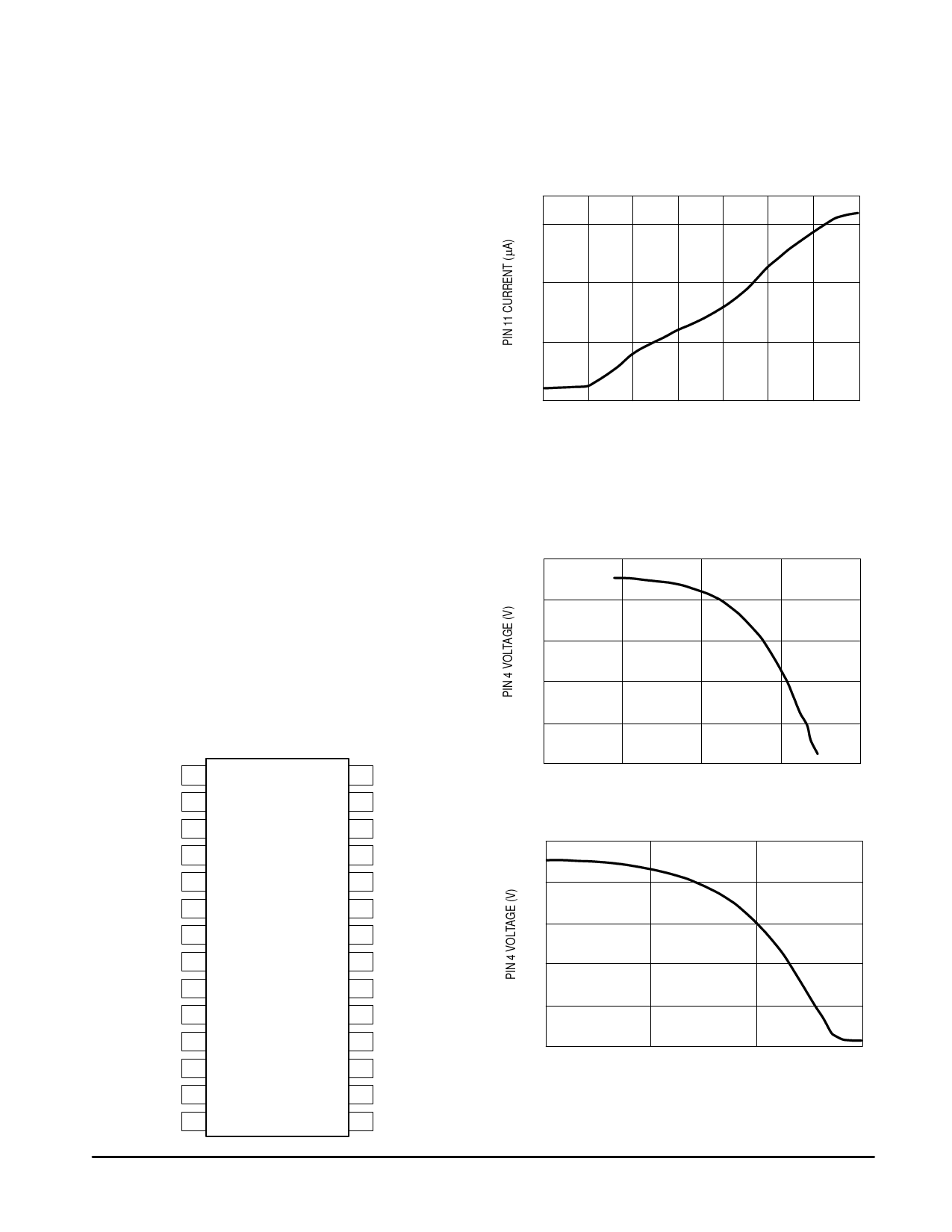
S Out versus IF Input:
The S output current at Pin 11 is provided by two
collectors, one a PNP source and the other a sink to ground.
The desired S output voltage can be selected using the curve
of Figure 3 and calculating the value of the required resistor.
Figure 3. S Output Current versus IF Input Level
70
60
40
20
0
30
40
50
60
70
80
90
100
IF INPUT LEVEL (dBµV)
RF FET AGC versus Mixer1 and Mixer2 Input Level:
Figures 4 and 5 are generated with no external resistance
on Pins 4 or 6, so they represent the minimum RF AGC
sensitivity of Mixer1 and Mixer2.
Figure 4. RF AGC Voltage versus Mixer1 Input
5.0
4.0
3.0
2.0
1.0
0
85
90
95
100
105
MIXER1 INPUT LEVEL (dBµV)
Figure 5. RF AGC Voltage versus Mixer2 Input
5.0
4.0
3.0
2.0
1.0
0
65
70
75
80
MIXER2 INPUT LEVEL (dBµV)
4
MOTOROLA ANALOG IC DEVICE DATA
Share Link: 