74LVC125APW-Q100J 데이터 시트보기 (PDF) - Nexperia B.V. All rights reserved
부품명
상세내역
제조사
74LVC125APW-Q100J
Nexperia B.V. All rights reserved

74LVC125APW-Q100J Datasheet PDF : 13 Pages
| |||
Nexperia
74LVC125A-Q100
Quad buffer/line driver with 5 V tolerant inputs/outputs; 3-state
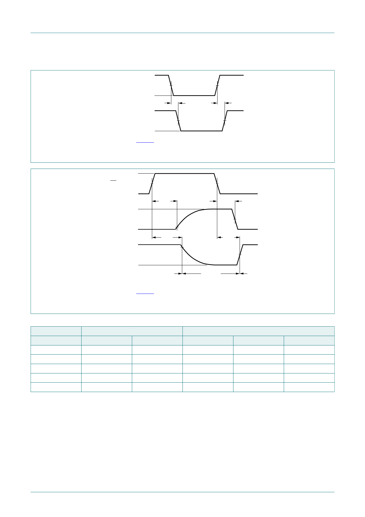
10.1. Waveforms and test circuit
VI
nA input
VM
GND
VOH
tPHL
tPLH
nY output
VM
Fig. 6.
VOL
mna230
Measurement points are given in Table 8.
VOL and VOH are typical output voltage levels that occur with the output load.
The input nA to output nY propagation delays
Fig. 7.
VI
nOE input
VM
GND
VCC
output
LOW-to-OFF
OFF-to-LOW
VOL
VOH
output
HIGH-to-OFF
OFF-to-HIGH
GND
tPLZ
tPZL
tPHZ
VX
VY
VM
tPZH
VM
outputs
enabled
outputs
disabled
outputs
enabled
mna362
Measurement points are given in Table 8.
VOL and VOH are typical output voltage levels that occur with the output load.
3-state enable and disable times
Table 8. Measurement points
Supply voltage Input
VCC
VI
1.2 V
VCC
1.65 V to 1.95 V VCC
2.3 V to 2.7 V
VCC
2.7 V
2.7 V
3.0 V to 3.6 V
2.7 V
VM
0.5 × VCC
0.5 × VCC
0.5 × VCC
1.5 V
1.5 V
Output
VM
0.5 × VCC
0.5 × VCC
0.5 × VCC
1.5 V
1.5 V
VX
VOL + 0.15 V
VOL + 0.15 V
VOL + 0.15 V
VOL + 0.3 V
VOL + 0.3 V
VY
VOH - 0.15 V
VOH - 0.15 V
VOH - 0.15 V
VOH - 0.3 V
VOH - 0.3 V
74LVC125A_Q100
Product data sheet
All information provided in this document is subject to legal disclaimers.
Rev. 2 — 5 May 2020
© Nexperia B.V. 2020. All rights reserved
6 / 13
Share Link: