AM26LS30FN 데이터 시트보기 (PDF) - Motorola => Freescale
부품명
상세내역
제조사
AM26LS30FN Datasheet PDF : 14 Pages
| |||
AM26LS30
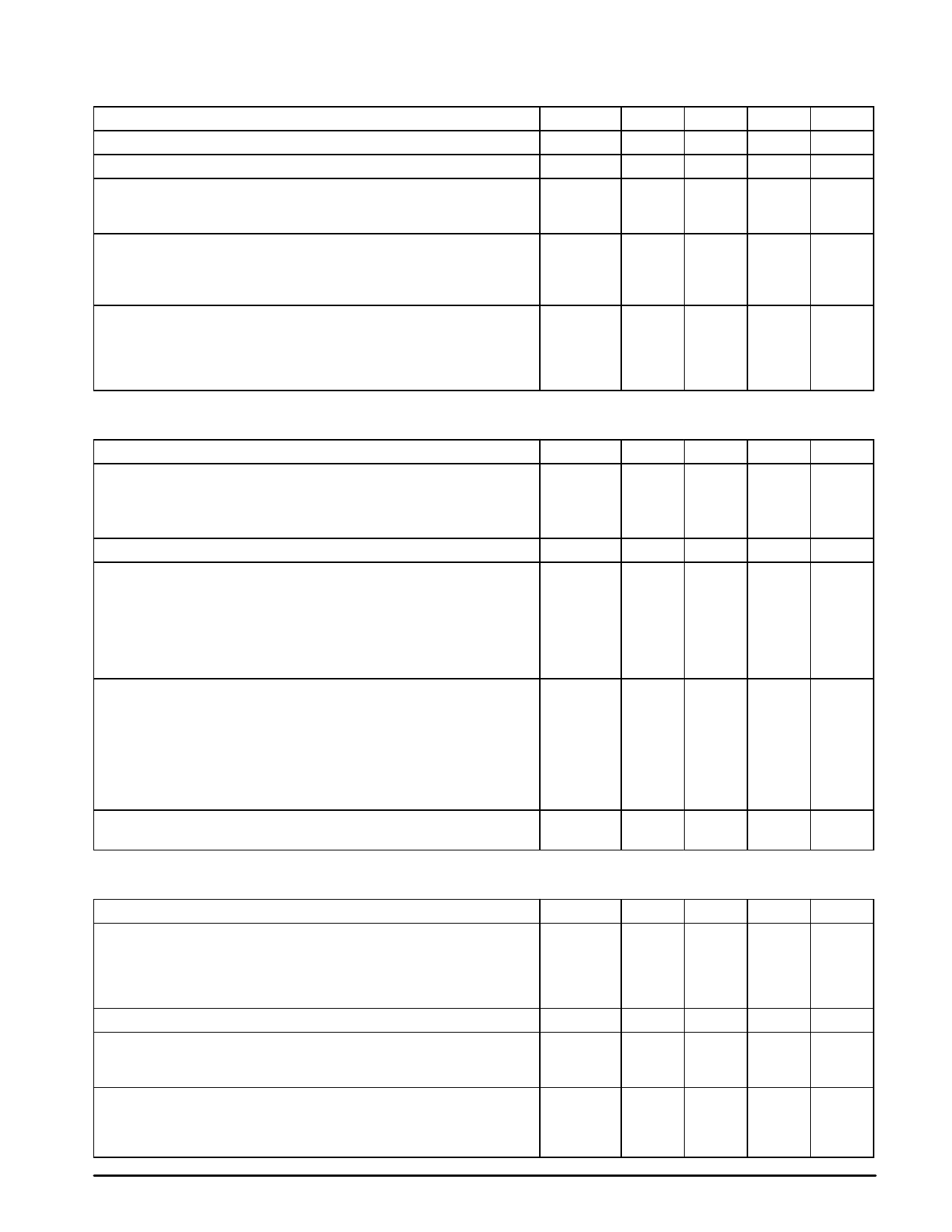
p TIMING CHARACTERISTICS (EIA–422–A differential mode, Pin 4 0.8 V, TA = 25°C, VCC = 5.0 V, VEE = Gnd, (Notes 1 and 3)
unless otherwise noted.)
Characteristic
Symbol
Min
Typ
Max
Unit
Differential Output Rise Time (Figure 3)
Differential Output Fall Time (Figure 3)
Propagation Delay Time – Input to Differential Output
Input Low to High (Figure 3)
Input High to Low (Figure 3)
tr
–
70
200
ns
tf
–
70
200
ns
ns
tPDH
–
90
200
tPDL
–
90
200
Skew Timing (Figure 3)
tPDH to tPDL for Each Driver
Max to Min tPDH Within a Package
Max to Min tPDL Within a Package
tSK1
tSK2
tSK3
ns
–
9.0
–
–
2.0
–
–
2.0
–
Enable Timing (Figure 4)
Enable to Active High Differential Output
Enable to Active Low Differential Output
Enable to 3–State Output From Active High
Enable to 3–State Output From Active Low
tPZH
tPZL
tPHZ
tPLZ
ns
–
150
300
–
190
350
–
80
350
–
110
300
q t t p ELECTRICAL CHARACTERISTICS (EIA–423–A single–ended mode, Pin 4 2.0 V, –40°C TA 85°C, 4.75 V VCC ,
p |VEE 5.25 V, (Notes 1 and 3) unless otherwise noted).
Characteristic
Symbol
Min
Typ
Max
Unit
Output Voltage (VCC = VEE = 4.75 V)
Single–Ended Voltage, RL = ∞ (Figure 2)
Single–Ended Voltage, RL = 450 Ω, (Figure 2)
Voltage Imbalance (Note 5), RL = 450 Ω
Vdc
VO1
4.0
4.2
6.0
VO2
3.6
3.95
6.0
∆VO2
–
0.05
0.4
Slew Control Current (Pins 16, 13, 12, 9)
ISLEW
–
±120
–
µA
p p Output Current (Each Output)
Power Off Leakage, VCC = VEE = 0, –6.0 V VO +6.0 V
Short Circuit Current (Output Short to Ground, Note 2)
p Vin 0.8 V (TA = 25°C)
p t t Vin 0.8 V (–40°C TA +85°C)
w Vin 2.0 V (TA = 25°C)
w t t Vin 2.0 V (–40°C TA +85°C)
IOLK
ISC+
ISC+
ISC–
ISC–
–100
0
+100
µA
60
80
150
mA
50
–
150
–150
–95
–60
–150
–
–50
Inputs
Low Level Voltage
High Level Voltage
Current @ Vin = 2.4 V
Current @ Vin = 15 V
p p Current @ Vin = 0.4 V
Current, 0 Vin 15 V, VCC = 0
Clamp Voltage (Iin = –12 mA)
VIL
VIH
IIH
IIHH
IIL
IIX
VIK
–
–
0.8
Vdc
2.0
–
–
Vdc
–
0
40
µA
–
0
100
–200
– 8.0
–
–
0
–
–1.5
–
–
Vdc
Power Supply Current (Outputs Open)
VCC = +5.25 V, VEE = –5.25 V, Vin = 0.4 V
ICC
–
17
30
mA
IEE
–22
– 8.0
–
q TIMING CHARACTERISTICS (EIA–423–A single–ended mode, Pin 4 2.0 V, TA = 25°C, VCC = 5.0 V, VEE = –5.0 V, (Notes 1 and 3)
unless otherwise noted.)
Characteristic
Symbol
Min
Typ
Max
Unit
Output Timing (Figure 5)
Output Rise Time, CC = 0
Output Fall Time, CC = 0
Output Rise Time, CC = 50 pF
Output Fall Time, CC = 50 pF
Rise Time Coefficient (Figure 16)
Propagation Delay Time, Input to Single Ended Output (Figure 5)
Input Low to High, CC = 0
Input High to Low, CC = 0
tr
tf
tr
tf
Crt
tPDH
tPDL
–
65
300
ns
–
65
300
–
3.0
–
µs
–
3.0
–
–
0.06
–
µs/pF
ns
–
100
300
–
100
300
Skew Timing, CC = 0 (Figure 5)
tPDH to tPDL for Each Driver
Max to Min tPDH Within a Package
Max to Min tPDL Within a Package
tSK4
tSK5
tSK6
ns
–
15
–
–
2.0
–
–
5.0
–
MOTOROLA ANALOG IC DEVICE DATA
3
Share Link: 