LT1313CS 데이터 시트보기 (PDF) - Linear Technology
부품명
상세내역
제조사
LT1313CS Datasheet PDF : 12 Pages
| |||
LT1313
ABSOLUTE MAXIMUM RATINGS
Supply Voltage ........................................................ 22V
Digital Input Voltage ........................ 7V to (GND – 0.3V)
Sense Input Voltage ......................... 7V to (GND – 0.3V)
VALID Output Voltage .................... 15V to (GND – 0.3V)
Output Short-Circuit Duration .......................... Indefinite
Operating Temperature ................................ 0°C to 70°C
Junction Temperature................................ 0°C to 125°C
Storage Temperature Range ..................–65°C to 150°C
Lead Temperature (Soldering, 10 sec).................. 300°C
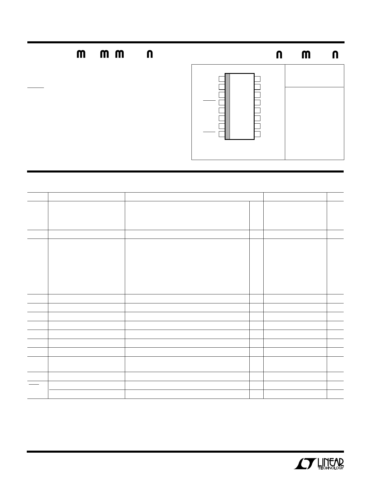
PACKAGE/ORDER INFORMATION
GND 1
AEN0 2
AEN1 3
AVALID 4
GND 5
BEN0 6
BEN1 7
BVALID 8
TOP VIEW
16 AVPPOUT
15 NC
14 VS
13 ASENSE
12 BVPPOUT
11 NC
10 VS
9 BSENSE
ORDER PART
NUMBER
LT1313CS
S PACKAGE
16-LEAD PLASTIC SO
TJMAX = 125°C, θJA = 100°C/ W
Consult factory for Industrial and Military grade parts.
ELECTRICAL CHARACTERISTICS VS = 13V to 20V, TA = 25°C (Note 1), unless otherwise noted.
SYMBOL PARAMETER
VPPOUT Output Voltage
ILKG
Output Leakage
IS
Supply Current
ILIM
VENH
VENL
IENH
IENL
VSEN5
VSEN3
ISEN
Current Limit
Enable Input High Voltage
Enable Input Low Voltage
Enable Input High Current
Enable Input Low Current
VCC Sense Threshold
VCC Sense Threshold
VCC Sense Input Current
VVALID TH
IVALID
VPPVALID Threshold Voltage
VPPVALIDOutput Drive Current
VPPVALID Output Leakage Current
CONDITIONS
Program to 12V, IOUT ≤ 120mA (Note 2)
q
Program to 5V, IOUT ≤ 30mA (Note 2)
q
Program to 3.3V, IOUT ≤ 30mA (Note 2)
q
Program to 0V, IOUT = – 300µA
Program to Hi-Z, 0V ≤ VPPOUT ≤ 12V
q
Both Channels Programmed to 0V
q
Both Channels Programmed to Hi-Z
q
One Channel Programmed to 12V, No Load (Note 3)
q
One Channel Programmed to 5V, No Load (Note 3)
q
One Channel Programmed to 3.3V, No Load (Note 3)
q
One Channel Programmed to 12V, IOUT = 120mA (Note 3) q
One Channel Programmed to 5V, IOUT = 30mA (Note 3) q
One Channel Programmed to 3.3V, IOUT = 30mA (Note 3) q
Program to 3.3V, 5V or 12V (Note 3)
q
q
2.4V ≤ VIN ≤ 5.5V
0V ≤ VIN ≤ 0.4V
VPPOUT = 3.3V to 5V (Note 4)
q
VPPOUT = 5V to 3.3V (Note 4)
q
VSENSE = 5V
VSENSE = 3.3V
Program to 12V, (Note 5)
q
Program to 12V, VVALID = 0.4V, (Note 5)
Program to 0V, VVALID = 12V, (Note 5)
MIN
11.52
4.75
3.135
– 10
2.4
TYP
12.00
5.00
3.30
0.42
60
60
260
105
85
126
31
31
330
20
0.01
3.60 4.05
3.60 4.00
38
18
10.5 11
1
3.3
0.1
MAX
12.48
5.25
3.465
0.60
10
100
100
400
150
120
132
33
33
500
0.4
50
1
4.50
4.50
60
30
11.5
10
UNITS
V
V
V
V
µA
µA
µA
µA
µA
µA
mA
mA
mA
mA
V
V
µA
µA
V
V
µA
µA
V
mA
µA
The q denotes the specifications which apply over the full operating
temperature range.
Note 1: Both VS pins (10, 14) must be connected together, and both
ground pins (1, 5) must be connected together.
Note 2: For junction temperatures greater than 110°C, a minimum
load of 1mA is recommended.
Note 3: The other channel is programmed to the 0V mode (XEN0 =
XEN1 = 0V) during this test.
Note 4: The VCC sense threshold voltage tests are performed
independently.
Note 5: The VPPVALID tests are performed independently.
2
Share Link: 