LT1313CS 데이터 시트보기 (PDF) - Linear Technology
부품명
상세내역
제조사
LT1313CS Datasheet PDF : 12 Pages
| |||

LT1313
APPLICATIONS INFORMATION
The fall time from 12V to 0V is set by the output capacitor
and an internal pull-down current source which sinks
about 30mA. This source will fully discharge a 1µF capaci-
tor in less than 1ms.
Thermal Considerations
Power dissipated by the device is the sum of two compo-
nents: output current multiplied by the input-output differ-
ential voltage: IOUT × (VIN – VOUT), and ground pin current
multiplied by supply voltage: (IGND × VIN).
The ground pin current can be found by examining the
Ground Pin Current curves in the Typical Performance
Characteristics section.
Heat sinking, for surface mounted devices, is accom-
plished by using the heat spreading capabilities of the PC
board and its copper traces.
The junction temperature of the LT1313 must be limited to
125°C to ensure proper operation. Use Table 1, in con-
junction with the typical performance graphs, to calculate
the power dissipation and die temperature for a particular
application and ensure that the die temperature does not
exceed 125°C under any operating conditions.
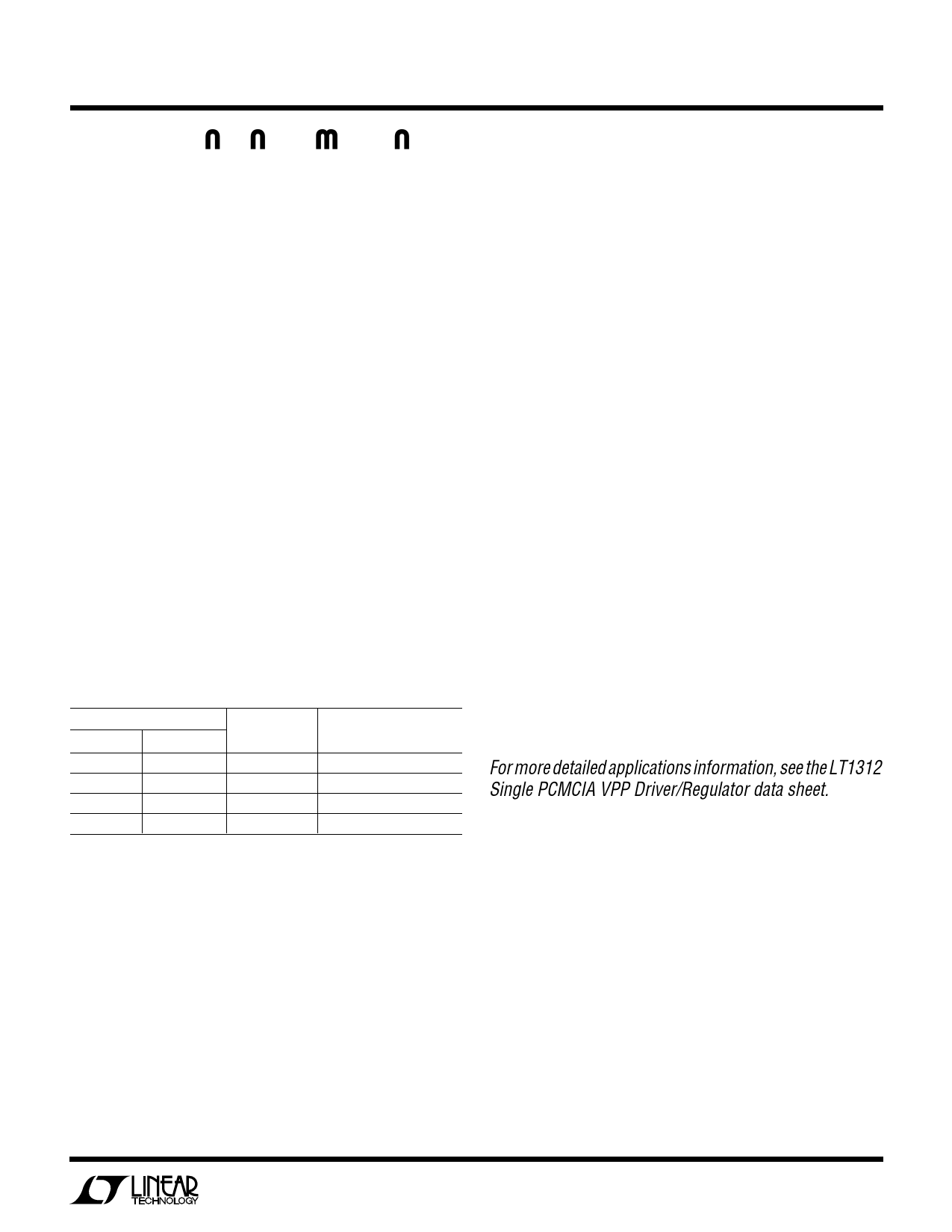
Table 1. 16-Pin SO Package*
COPPER AREA
TOPSIDE
BACKSIDE BOARD AREA
2500 sq mm 2500 sq mm 2500 sq mm
1000 sq mm 2500 sq mm 2500 sq mm
225 sq mm 2500 sq mm 2500 sq mm
1000 sq mm 1000 sq mm 1000 sq mm
* Device is mounted on topside.
THERMAL RESISTANCE
(JUNCTION-TO-AMBIENT)
120°C/ W
120°C/ W
125°C/ W
131°C/ W
Calculating Junction Temperature
Example: given an output voltage of 12V, an input supply
voltage of 14V, and an output current of 100mA (one VPP
output), and a maximum ambient temperature of 50°C,
what will the maximum junction temperature be?
Power dissipated by the device will be equal to:
IOUT × (VS – VPPOUT) + (IGND × VIN)
where,
IOUT = 100mA
VIN = 14V
IGND at (IOUT = 100mA, VIN = 14V) = 5mA
so,
PD = 100mA × (14V –12V) + (5mA × 15V) = 0.275W
Using Table 1, the thermal resistance will be in the range
of 120°C/W to 131°C/W depending upon the copper area.
So the junction temperature rise above ambient will be
less than or equal to:
0.275W × 131°C/W = 36°C
The maximum junction temperature will then be equal to
the junction temperature rise above ambient plus the
maximum ambient temperature or:
TJMAX = 50°C + 36°C = 86°C
For more detailed applications information, see the LT1312
Single PCMCIA VPP Driver/Regulator data sheet.
7