MAX987 데이터 시트보기 (PDF) - Maxim Integrated
부품명
상세내역
제조사
MAX987 Datasheet PDF : 13 Pages
| |||
High-Speed, Micropower, Low-Voltage,
SOT23, Rail-to-Rail I/O Comparators
ABSOLUTE MAXIMUM RATINGS
Supply Voltage (VCC to VEE) ...................................................6V
IN_-, IN_+ to VEE .......................................-0.3V to (VCC + 0.3V)
Current into Input Pins .....................................................±20mA
OUT_ to VEE
MAX987/MAX991/MAX995 ....................-0.3V to (VCC + 0.3V)
MAX988/MAX992/MAX996 ..................................-0.3V to +6V
OUT_ Short-Circuit Duration to VEE or VCC ...........................10s
Continuous Power Dissipation (TA = +70°C)
5-Pin SC70 (derate 3.1mW/°C above +70°C) ...............247mW
5-Pin SOT23 (derate 7.10mW/°C above +70°C)...........571mW
8-Pin SOT23 (derate 9.1mW/°C above +70°C).............727mW
8-Pin SO (derate 5.88mW/°C above +70°C).................471mW
8-Pin µMAX (derate 4.5mW/°C above +70°C) ..............362mW
14-Pin TSSOP (derate 9.1mW/°C above +70°C) ..........727mW
14-Pin SO (derate 8.33mW/°C above +70°C)...............667mW
Operating Temperature Range ...........................-40°C to +85°C
Storage Temperature Range .............................-65°C to +150°C
Lead Temperature (soldering, 10s) .................................+300°C
Stresses beyond those listed under “Absolute Maximum Ratings” may cause permanent damage to the device. These are stress ratings only, and functional
operation of the device at these or any other conditions beyond those indicated in the operational sections of the specifications is not implied. Exposure to
absolute maximum rating conditions for extended periods may affect device reliability.
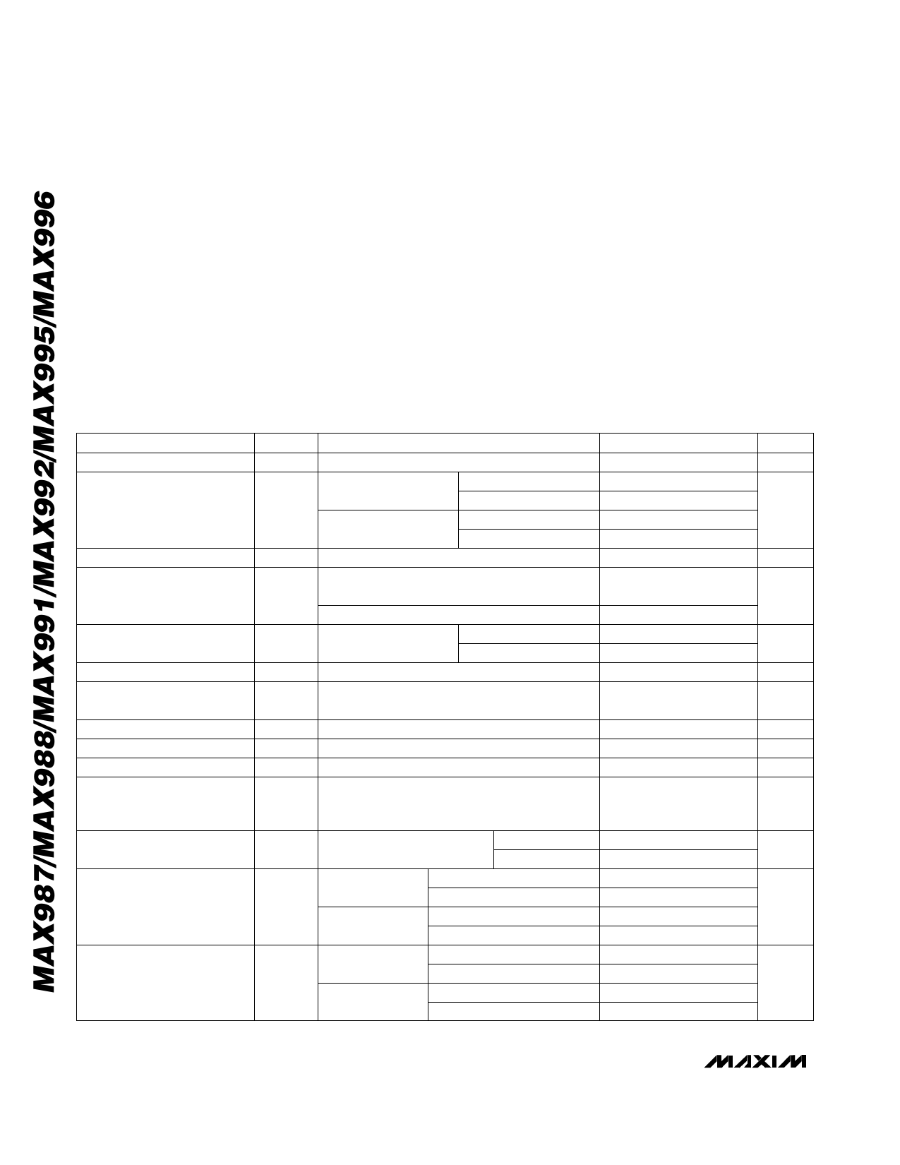
ELECTRICAL CHARACTERISTICS (Note 1)
(VCC = +2.7V to +5.5V, VEE = 0V, VCM = 0V, TA = -40°C to +85°C, unless otherwise noted. Typical values are at TA = +25°C.)
PARAMETER
Supply Voltage
Supply Current per
Comparator
Power-Supply Rejection Ratio
SYMBOL
VCC
ICC
PSRR
CONDITIONS
Inferred from PSRR test
VCC = 5V
TA = +25°C
TA = -40°C to +85°C
VCC = 2.7V
TA = +25°C
TA = -40°C to +85°C
2.5V ≤ VCC ≤ 5.5V
Common-Mode Voltage
Range (Note 2)
Input Offset Voltage
(Note 3)
Input Hysteresis
Input Bias Current
(Note 4)
VCMR
VOS
VHYST
IB
TA = +25°C
TA = -40°C to +85°C
Full common-mode
range
TA = +25°C
TA = -40°C to +85°C
MIN
2.5
55
VEE -
0.25
VEE
TYP
53
48
80
±0.5
±2.5
MAX
5.5
80
96
80
96
VCC +
0.25
VCC
±5
±7
UNITS
V
µA
dB
V
mV
mV
0.001 10
nA
Input Offset Current
Input Capacitance
Common-Mode Rejection Ratio
IOS
CIN
CMRR
0.5
pA
1.0
pF
50
80
dB
Output Leakage Current
(MAX988/MAX992/
MAX996 only)
ILEAK VOUT = high
1.0
µA
Output Short-Circuit Current
OUT Output-Voltage Low
OUT Output-Voltage High
(MAX987/MAX991/
MAX995 Only)
ISC
VOL
VOH
Sourcing or sinking,
VOUT = VEE or VCC
VCC = 5V
VCC = 2.7V
VCC = 5V,
ISINK = 8mA
TA = +25°C
TA = -40°C to +85°C
VCC = 2.7V,
ISINK = 3.5mA
TA = +25°C
TA = -40°C to +85°C
VCC = 5V,
ISOURCE = 8mA
TA = +25°C
TA = -40°C to +85°C
VCC = 2.7V,
TA = +25°C
ISOURCE = 3.5mA TA = -40°C to +85°C
95
mA
35
0.2
0.4
0.55
V
0.15
0.3
0.4
4.6
4.85
4.45
V
2.4
2.55
2.3
2 _______________________________________________________________________________________
Share Link: 