MAX987 데이터 시트보기 (PDF) - Maxim Integrated
부품명
상세내역
제조사
MAX987 Datasheet PDF : 13 Pages
| |||
High-Speed, Micropower, Low-Voltage,
SOT23, Rail-to-Rail I/O Comparators
Detailed Description
The MAX987/MAX988/MAX991/MAX992/MAX995/
MAX996 are single/dual/quad low-power, low-voltage
comparators. They have an operating supply voltage
range between +2.5V and +5.5V and consume only
48µA per comparator, while achieving 120ns propaga-
tion delay. Their common-mode input voltage range
extends 0.25V beyond each rail. Internal hysteresis
ensures clean output switching, even with slow-moving
input signals. Large internal output drivers allow rail-to-
rail output swing with up to 8mA loads.
The output stage employs a unique design that mini-
mizes supply-current surges while switching, virtually
eliminating the supply glitches typical of many other
comparators. The MAX987/MAX991/MAX995 have a
push-pull output structure that sinks as well as sources
current. The MAX988/MAX992/MAX996 have an open-
drain output stage that can be pulled beyond VCC to an
absolute maximum of 6V above VEE.
Input Stage Circuitry
The devices’ input common-mode range extends from
-0.25V to (VCC + 0.25V). These comparators may oper-
ate at any differential input voltage within these limits.
Input bias current is typically 1.0pA if the input voltage
is between the supply rails. Comparator inputs are pro-
tected from overvoltage by internal body diodes con-
nected to the supply rails. As the input voltage exceeds
the supply rails, these body diodes become forward
biased and begin to conduct. Consequently, bias cur-
rents increase exponentially as the input voltage
exceeds the supply rails.
Output Stage Circuitry
These comparators contain a unique output stage
capable of rail-to-rail operation with up to 8mA loads.
Many comparators consume orders of magnitude more
current during switching than during steady-state oper-
ation. However, with this family of comparators, the
supply-current change during an output transition is
extremely small. The Typical Operating Characteristics
Supply Current vs. Output Transition Frequency graph
shows the minimal supply-current increase as the out-
put switching frequency approaches 1MHz. This char-
acteristic eliminates the need for power-supply filter
capacitors to reduce glitches created by comparator
switching currents. Battery life increases substantially
in high-speed, battery-powered applications.
Applications Information
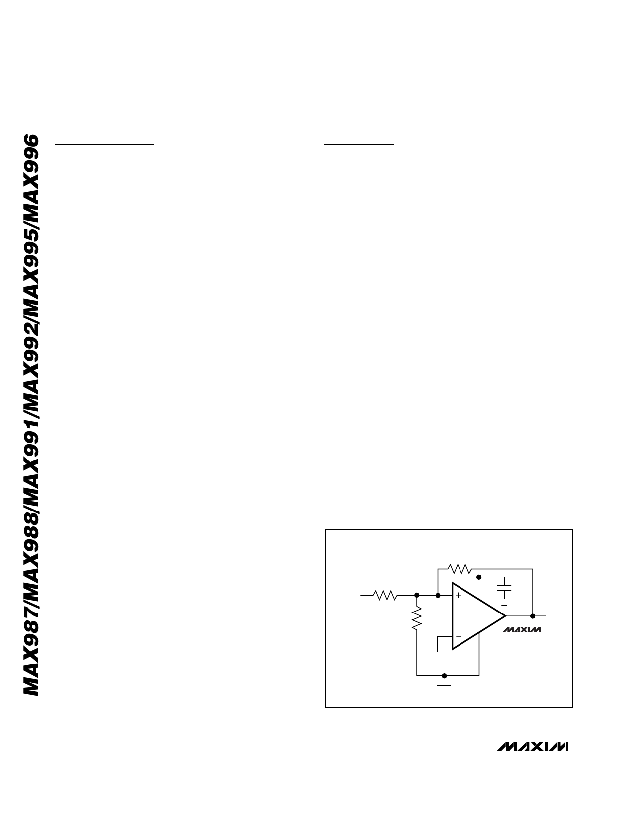
Additional Hysteresis
MAX987/MAX991/MAX995
The MAX987/MAX991/MAX995 have ±2.5mV internal
hysteresis. Additional hysteresis can be generated with
three resistors using positive feedback (Figure 1).
Unfortunately, this method also slows hysteresis
response time. Use the following procedure to calcu-
late resistor values for the MAX987/MAX991/MAX995.
1) Select R3. Leakage current at IN is under 10nA;
therefore, the current through R3 should be at least
1µA to minimize errors caused by leakage current.
The current through R3 at the trip point is (VREF -
VOUT) / R3. Considering the two possible output
states and solving for R3 yields two formulas: R3 =
VREF / 1µA or R3 = (VREF - VCC) / 1µA. Use the
smaller of the two resulting resistor values. For
example, if VREF = 1.2V and VCC = 5V, then the two
R3 resistor values are 1.2MΩ and 3.8MΩ. Choose a
1.2MΩ standard value for R3.
2) Choose the hysteresis band required (VHB). For this
example, choose 50mV.
3) Calculate R1 according to the following equation:
R1 = R3 x (VHB / VCC)
For this example, insert the values R1 = 1.2MΩ x
(50mV / 5V) = 12kΩ.
4) Choose the trip point for VIN rising (VTHR; VTHF is
the trip point for VIN falling). This is the threshold
voltage at which the comparator switches its output
from low to high as VIN rises above the trip point. For
this example, choose 3V.
VCC
R3
R1
VIN
R2
VREF
0.1µF
VCC
OUT
VEE
MAX987
MAX991
MAX995
Figure 1. Additional Hysteresis (MAX987/MAX991/MAX995)
8 _______________________________________________________________________________________
Share Link: 