A49LF004 데이터 시트보기 (PDF) - AMIC Technology
부품명
상세내역
제조사
A49LF004 Datasheet PDF : 32 Pages
| |||
A49LF004
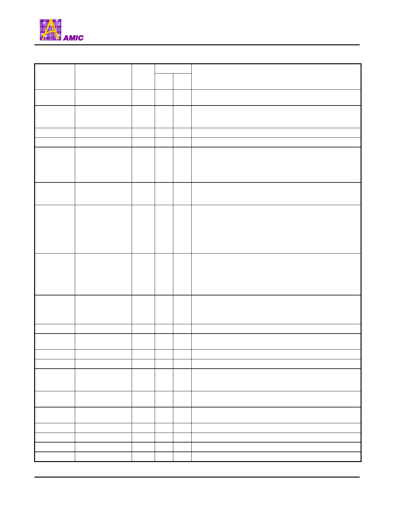
Table 1: Pin Description
Symbol
A10-A0
I/O7-I/O0
OE#
WE#
IC
INIT#
ID[3:0]
FGPI[4:0]
TBL#
FWH[3:0]
CLK
FWH4
Pin Name
Address
Data
Output Enable
Write Enable
Interface
Configuration Pin
Initialize
Identification Inputs
General Purpose
Inputs
Top Block Lock
FWH I/Os
Clock
FWH Input
Type
IN
I/O
IN
IN
IN
IN
IN
IN
IN
I/O
IN
IN
Interface
A/A
Mux
FWH
Descriptions
X
Inputs for addresses during Read and Write operations in A/A
Mux mode. Row and column addresses are latched by R/C# pin.
To output data during Read cycle and receive input data during
X
Write cycle in A/A Mux mode. The outputs are in tri-state when
OE# is high.
X
To control the data output buffers.
X
To control the Write operations.
To determine which interface is operational. When held high, A/A
Mux mode is enabled and when held low, FWH mode is enabled.
X X This pin must be setup at power-up or before return from reset
and not change during device operation. This pin is internally
pulled down with a resistor between 20-100 KΩ.
This is the second reset pin for in-system use. INIT# and RST#
X pins are internally combined and initialize a device reset when
driven low.
These four pins are part of the mechanism that allows multiple
FWH devices to be attached to the same bus. To identify the
component, the correct strapping of these pins must be set. The
X boot device must have ID[3:0]=0000 and it is recommended that
all subsequent devices should use sequential up-count
strapping. These pins are internally pulled down with a resistor
between 20-100 KΩ.
These individual inputs can be used for additional board
flexibility. The state of these pins can be read immediately at
X
boot, through FWH internal registers. These inputs should be at
their desired state before the start of the PCI clock cycle during
which the read is attempted, and should remain in place until the
end of the Read cycle. Unused FGPI pins must not be floated.
To prevent any write operations to the Boot Block when driven
X
low, regardless of the state of the block lock registers. When
TBL# is high it disables hardware write protection for the top
Boot Block. This pin cannot be left unconnected.
X I/O Communications in FWH mode.
X
To provide a clock input to the device. This pin is the same as
that for the PCI clock and adheres to the PCI specifications.
X Input communication in FWH mode.
RST#
WP#
Reset
Write Protect
IN
X
IN
R/C#
Row/Column Select IN
X
RB#
Ready/Busy#
OUT X
RES
Reserved
VDD
Power Supply
PWR X
VSS
Ground
PWR X
NC
No Connection
X
1. IN=Input, OUT=output, I/O=Input/Output, PWR=Power
X To reset the operation of the device
When low, prevents any write operations to all but the highest
X addressable block. When WP# is high it disables hardware write
protection for these blocks. This pin cannot be left unconnected.
This pin determines whether the address pins are pointing to the
row addresses or the column addresses in A/A Mux mode.
To determine if the device is busy in write operations. Valid only
in A/A Mux mode.
X Reserved. These pins must be left unconnected.
X To provide power supply (3.0-3.6Volt).
X Circuit ground. All VSS pins must be grounded.
X Unconnected pins.
PRELIMINARY (November, 2003, Version 0.0)
4
AMIC Technology, Corp.
Share Link: 