AD9040A(RevD) 데이터 시트보기 (PDF) - Analog Devices
부품명
상세내역
제조사
AD9040A Datasheet PDF : 16 Pages
| |||
AD9040A
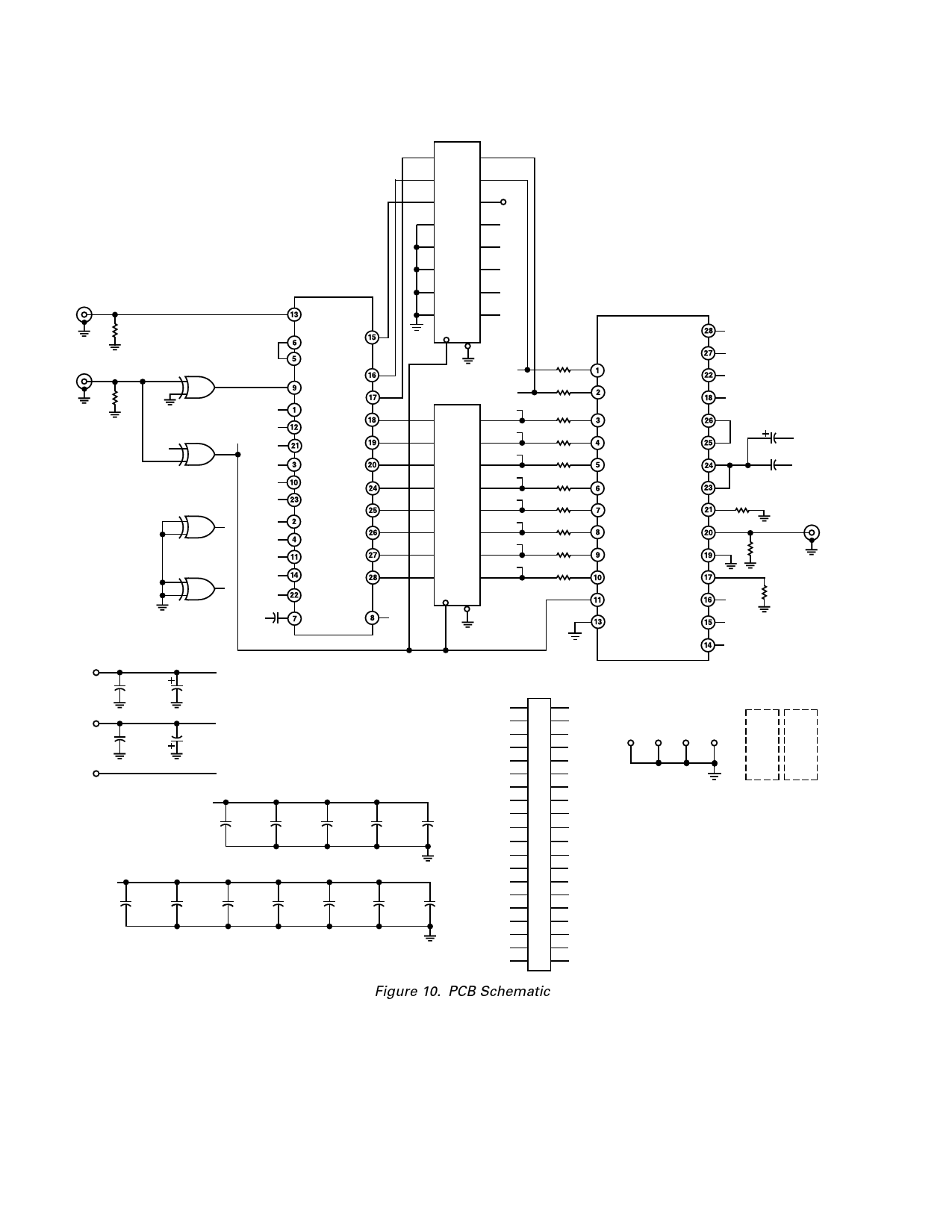
Layout Information
performance without (or prior to) developing a user-specific
Preserving the accuracy and dynamic performance of the
printed circuit board. The two-sided board includes a recon-
AD9040A requires that designers pay special attention to the
layout of the printed circuit board.
struction DAC and digital output interface and uses the layout
and applications suggestions outlined above. It is available from
Analog paths should be kept as short as possible and be properly Analog Devices at nominal cost.
terminated to avoid reflections. The analog input and reference Generous space is provided near the analog input and digital
voltage connections should be kept away from digital signal
paths; this reduces the amount of digital switching noise that is
outputs to support any additional signal processing components
the user may wish to add. This prototyping area includes through-
capacitively coupled into the analog section. Digital signal paths
should also be kept short and run lengths should be matched to
holes with 100-mil centers to support a variety of component
additions.
avoid propagation delay mismatch. The AD9040A digital out-
puts should be buffered or latched close to the device (<2 cm).
This prevents load transients, which may feed back into the device.
Input/Output/Supply Information
Power supply, analog input, clock connections, and reconstructed
output (RC OUTPUT) are identified by labels on the evalua-
OBSOLETE In high speed circuits, layout of the ground is critical. A single,
low impedance ground plane on the component side of the
board is recommended. Power supplies should be capacitively
coupled to the ground plane with high quality chip capacitors to
reduce noise in the circuit. Multilayer boards allow designers to
lay out signal traces without interrupting the ground plane and
provide low impedance ground planes. In systems with dedi-
cated analog and digital grounds, all grounds of the AD9040A
should be connected to the analog ground plane.
The power supplies of the AD9040A should be isolated from
the supplies used for external devices; this reduces the amount
of noise coupled into the ADC. The digital 5 V connection of
the device (VD, Pin 23) powers the digital outputs and should
be connected to the same supply as +VS (Pins 3 and 10). Con-
necting VD to a system digital supply may couple noise into the
device. Sockets limit dynamic performance and are not recom-
mended for use with the AD9040A.
tion board. Operation of the evaluation board should conform
to the following characteristics.
Table I. Evaluation Board Characteristics
Parameter
Supply Current
+5 V
–5.2 V
AIN
Impedance
Voltage Range
CLOCK
Impedance
Frequency
RC OUTPUT
Impedance
Typical
250
300
51
± 1.0
51
40
51
Unit
mA
mA
Ω
V
Ω
MSPS
Ω
Voltage Range
0 V to –1 V
V
EVALUATION BOARD
The evaluation board for the AD9040A (AD9040A/PCB) pro-
vides an easy and flexible method for evaluating the ADC’s
Analog Input
Analog input signals can be fed directly into the device under
test input (AIN). The AIN input is terminated at the device with
a 51 Ω resistor.
–10–
REV. D
Share Link: 