AD9040A(RevD) 데이터 시트보기 (PDF) - Analog Devices
부품명
상세내역
제조사
AD9040A Datasheet PDF : 16 Pages
| |||
AD9040A
ABSOLUTE MAXIMUM RATINGS1
± VS . . . . . . . . . . . . . . . . . . . . . . . . . . . . . . . . . . . . . . . ± 7 V
VD . . . . . . . . . . . . . . . . . . . . . . . . . . . . . . . . . . . . . . . . 7 V
Analog Inputs . . . . . . . . . . . . . . . . . . . . . . . . . . . . –VS to +VS
Digital Inputs . . . . . . . . . . . . . . . . . . . . . . . . . . . . 0 V to +VS
VREF Input . . . . . . . . . . . . . . . . . . . . . . . . . . . . . . . 0 V to +VS
Digital Output Current . . . . . . . . . . . . . . . . . . . . . . . . . 20 mA
Operating Temperature
AD9040AJN/AD9040AJR . . . . . . . . . . . . . . . . . 0°C to 70°C
Storage Temperature . . . . . . . . . . . . . . . . . –65°C to +150°C
Maximum Junction Temperature2 (JN/JR Suffixes) . . . . 150°C
Lead Soldering Temp (10 sec) . . . . . . . . . . . . . . . . . . . . 300°C
NOTES
1Absolute maximum ratings are limiting values to be applied individually and
beyond which the serviceability of the circuit may be impaired. Functional
operability is not necessarily implied. Exposure to absolute maximum rating
conditions for an extended period of time may affect device reliability.
2Typical thermal impedances (parts soldered to board):
N Package (PDIP): JA = 42°C/W; JC = 10°C/W.
R Package (SOIC): JA = 47°C/W; JC = 10°C/W.
ORDERING GUIDE
OBSOLETE Model
AD9040AJN
AD9040AJR
AD9040AJR-REEL
Temperature Range
0°C to 70°C
0°C to 70°C
0°C to 70°C
Package Description
28-Lead PDIP
28-Lead SOIC Package
28-Lead SOIC Package
CAUTION
ESD (electrostatic discharge) sensitive device. Electrostatic charges as high as 4000 V readily
accumulate on the human body and test equipment and can discharge without detection. Although the
AD9040A features proprietary ESD protection circuitry, permanent damage may occur on devices
subjected to high energy electrostatic discharges. Therefore, proper ESD precautions are recommended
to avoid performance degradation or loss of functionality.
Package Option
N-28
R-28
R-28
N
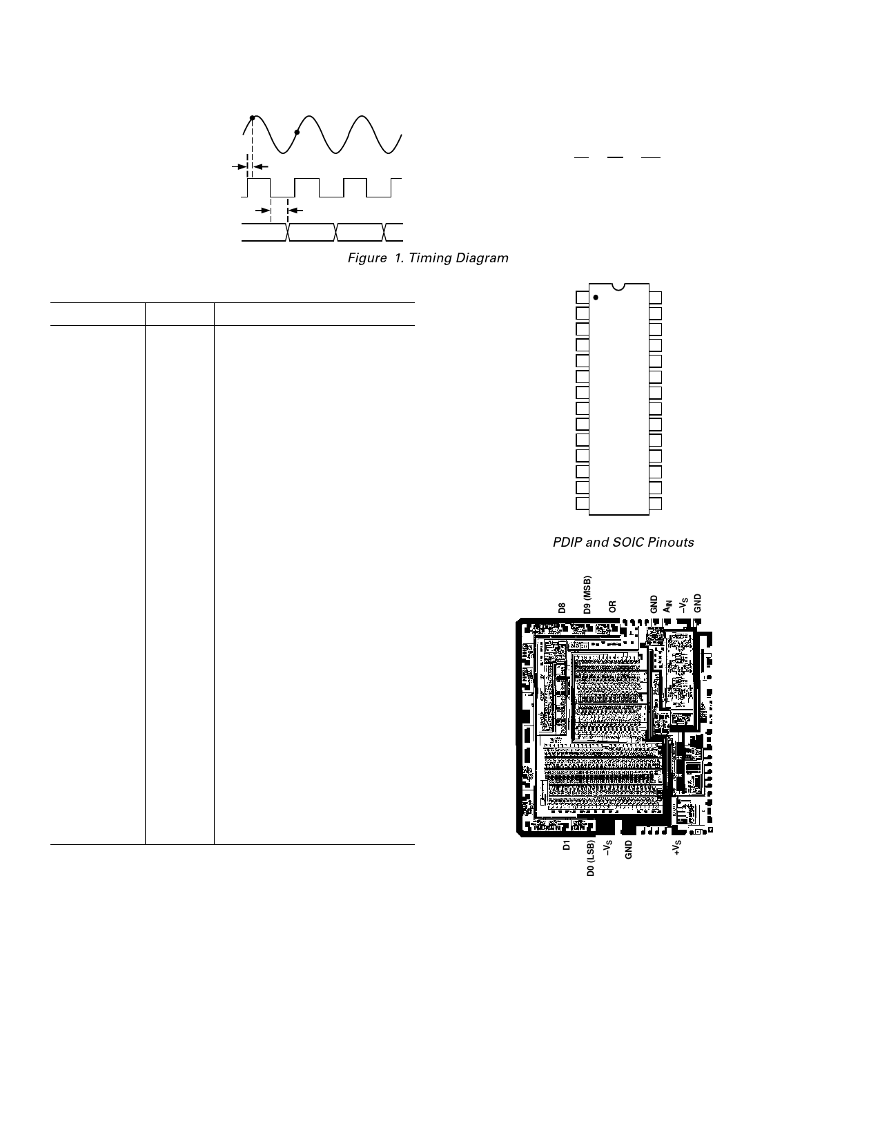
AIN
N+1
ENCODE
DIGITAL
OUTPUTS
tA NO. 2
tEH tEL
tPD
N–3
N–2
NO. 3
N–1
SYMBOL
tA
tEH
tEL
tPD
DESCRIPTION
APERTURE DELAY
PULSEWIDTH HIGH
PULSEWIDTH LOW
OUTPUT PROP DELAY
MIN
10ns
10ns
7.5ns
TYP
1.9ns
10ns
MAX
100ns
100ns
12ns
Figure 1. Timing Diagram
–4–
REV. D
Share Link: 