LC7073 데이터 시트보기 (PDF) - SANYO -> Panasonic
부품명
상세내역
제조사
LC7073 Datasheet PDF : 9 Pages
| |||
LC7073, 7073M
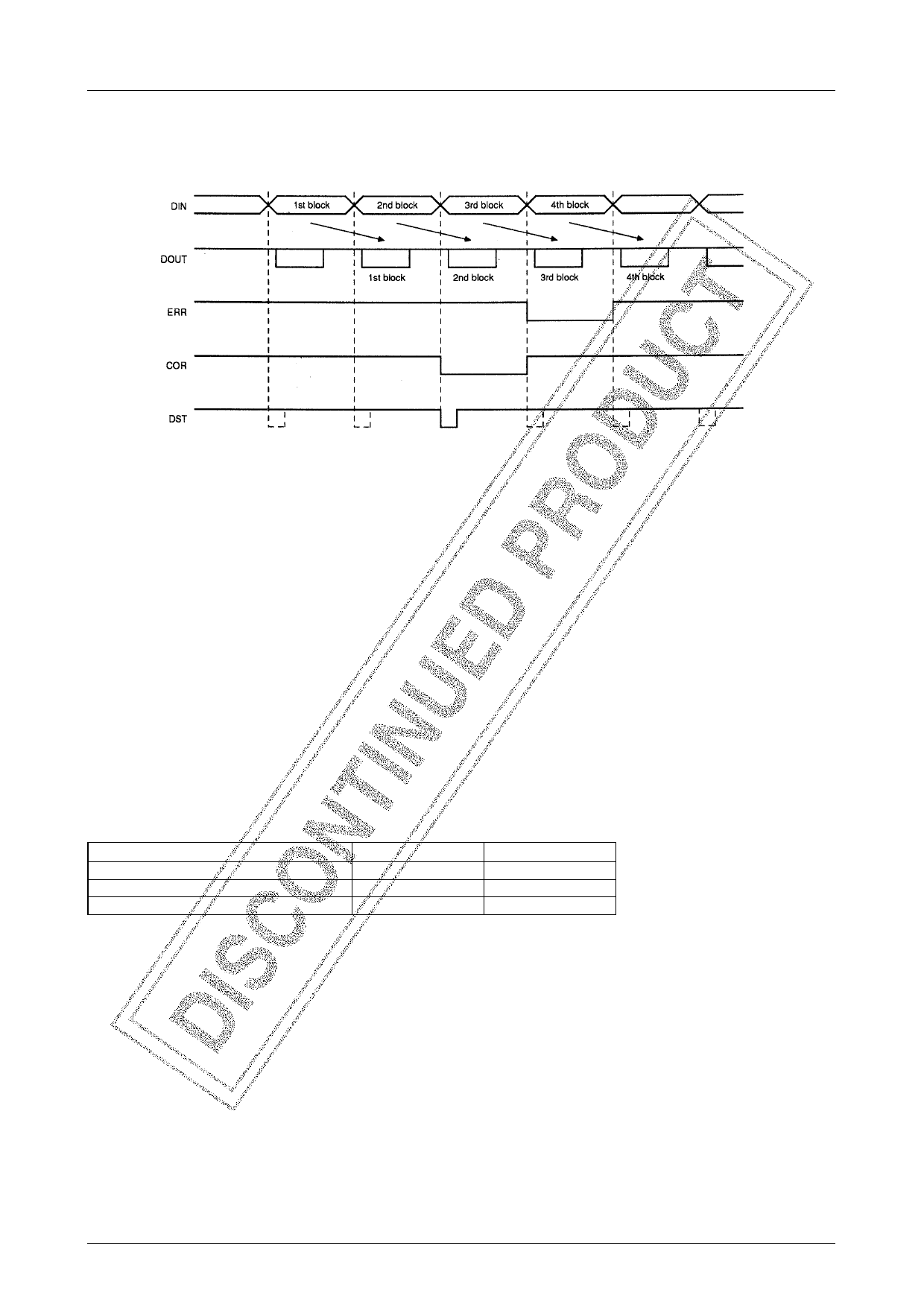
Timing Diagrams
The relationship between the LC7073 and LC7073M input data (RDS demodulated data output) and output data is shown
in figure 1.
Figure 1. Input and output data
Note
The dotted lines show data start (DST) pulses when the data start control (DSTCTL) is LOW. The serial output data is
delayed by one block between input and output. The error (ERR) and correction (COR) signals remain active if errors are
detected continually.
Serial Output Data Timing and Format
The following list shows the symbols used in the serial output data string in figure 2.
S
E
F
OE
OF
A/B
B0, B1
D0 to D15
Start bit (normally 0)
Error flag (See table 1.)
Correction flag (See table 1.)
Offset E (normally 0, not used)
Offset F (normally 0, not used)
Group. 0–group A, 1–group B
Block bits. 00–1st block, 01–2nd block, 10–3rd block, 11–4th block
Output data
Table 1. Error and correction flags
No error
Error corrected
Not correctable
Indication
E
F
0
0
0
1
1
×
Note
× = don’t care
No.3932–5/9
Share Link: 