AMSOP-07 데이터 시트보기 (PDF) - Advanced Monolithic Systems Inc
부품명
상세내역
제조사
AMSOP-07 Datasheet PDF : 6 Pages
| |||
AMSOP-07
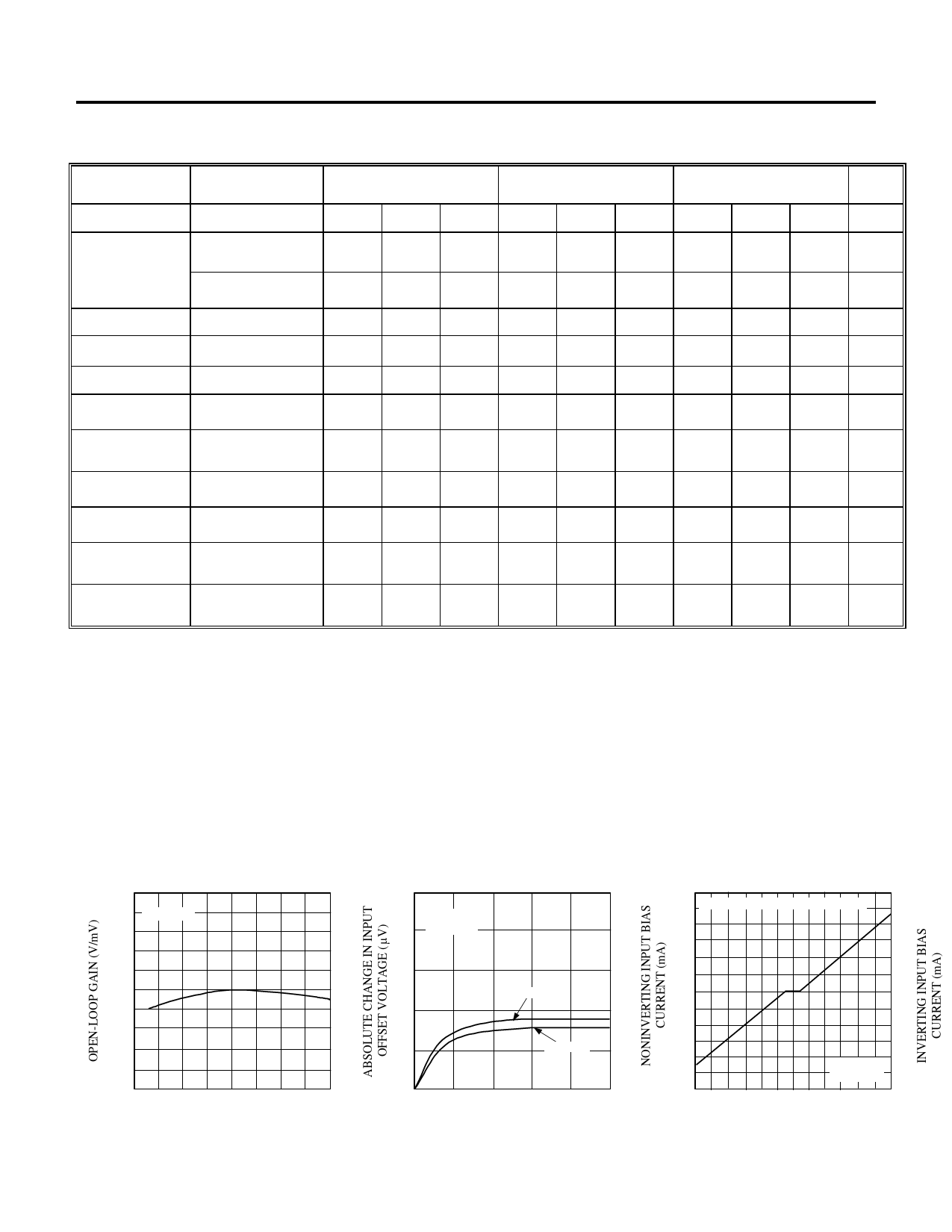
ELECTRICAL CHARACTERISTICS
Electrical Characteristics at VIN= ±15, at -40°C ≤ TA ≤ +85°C unless otherwise specified.
Parameter
Conditions
AMSOP-07E
AMSOP-07 C
Min Typ Max Min Typ Max
Input Offset Voltage (Note 2)
45
130
85
250
Average Input
Offset
Voltage Drift
(Note 5)
Input Offset Current
Average Input
Offset Current Drift
Input Bias Current
Without External Trim
With External Trim
RP =2kΩ
(Note 4)
Average Input Bias (Note 4)
Current Drift
Input Voltage
± 13
Range
Common-Mode
VCM = ± 13
103
Rejection Ratio
Power Supply
Rejection Ratio
VS = ± 13 to ± 18
Large-Signal
Voltage Gain
RL≥2kΩ, VO =± 10V
180
0.3
0.3
0.9
8
± 1.5
13
± 13.5
123
7
450
1.3
1.3
5.3
35
± 5.5
35
32
0.5
1.8
0.4
1.6
1.6
12
± 2.2
18
8.0
50
± 9.0
50
± 13 ± 13.5
97
120
10
51
100
400
Output Voltage
Swing
RL ≥2kΩ
± 12.0 ± 13.0
± 12.0 ± 13.0
AMSOP-07 D
Min Typ Max
85
250
0.7
2.5
Units
µV
µV/°C
0.7
2.5
µV/°C
1.6
12
± 3.0
18
8.0
nA
50
pA/°C
± 14
nA
50
pA/°C
± 13 ± 13.5
V
94
106
10
100
400
dB
51
µV/V
V/mV
± 12.0 ± 13.0
V
Note 1: Absolute Maximum Ratings indicate limits beyond which damage to the device may occur. Operating Ratings indicate conditions for which the
device is intended to be functional, but do not guarantee specific performance limits. For guaranteed specifications and test conditions, see the Electrical
Characteristics. The guaranteed specifications apply only for the test conditions listed.
Note 2: Input Offset Voltage measurements are performed by automated test equipment approximately 0.5 seconds after application of power.
Note 3: Long-Term Input Offset Voltage Stability refers to the averaged trend line of VOS vs. Time over extended periods after the first 30 days of operation.
Excluding the initial hour of operation, changes in VOS during the first 30 operating days are typically 2.5µV. Parameter is sample tested.
Note 4: Sample tested
Note 5: Guaranteed by design.
Note 6: Guaranteed but not tested.
TYPICAL PERFORMANCE CHARACTERISTICS
1000
800
Open-Loop Gain vs Temperature
VS = ±15V
Warm-UpDrift
25
TA = 25° C
20
VS = ±15V
600
15
OP-07C
400
10
200
5
OP-07E
0
-50
0
50
TEMPERATURE (° C)
0
100
0
1
23
4
5
TIME AFTER POWER SUPPLY TURN-ON (minutes)
Input Bias Current vs
Differrential Input Voltage
30
-30
AT | VDIFF | ≤ 1.0V, | IB | ≤ 7nA (OP-07C)
20
-20
10
-10
0
0
-10
10
-20
VS = ±15V
20
TA = 25° C
-30
30
-30 -20 -10 0 10 20 30
DIFFERENTIAL INPUT VALUE (V)
Advanced Monolithic Systems, Inc. www.advanced-monolithic.com Phone (925) 443-0722 Fax (925) 443-0723
Share Link: 