ATC25 데이터 시트보기 (PDF) - Atmel Corporation
부품명
상세내역
제조사
ATC25 Datasheet PDF : 11 Pages
| |||
Features
• Comprehensive Library of Standard Logic Cells
• ATC25 I/O Cells Designed to Operate with VDD = 2.5V ± 0.25V as Main Target Operating
Conditions
• IO33 Pad Library Provides Interface to 3V Environment
• Oscillators Provide Stable Clock Sources
• Basic Analog Input/Output, Power, Ground and Multiplexer Cells Available,
High-performance Analog Cells Can Be Developed on Request
• Memory Cells Compiled to the Precise Requirements of the Design
• Compatible with Atmel’s Extensive Range of Microcontroller, DSP, Standard Interface
and Application Specific Cells
Description
The Atmel ATC25 CBIC family is fabricated on a proprietary 0.25 micron five-layer-
metal CMOS process intended for use with a supply voltage of 2.5V ± 0.25V. The fol-
lowing table shows the range for which Atmel library cells have been characterized.
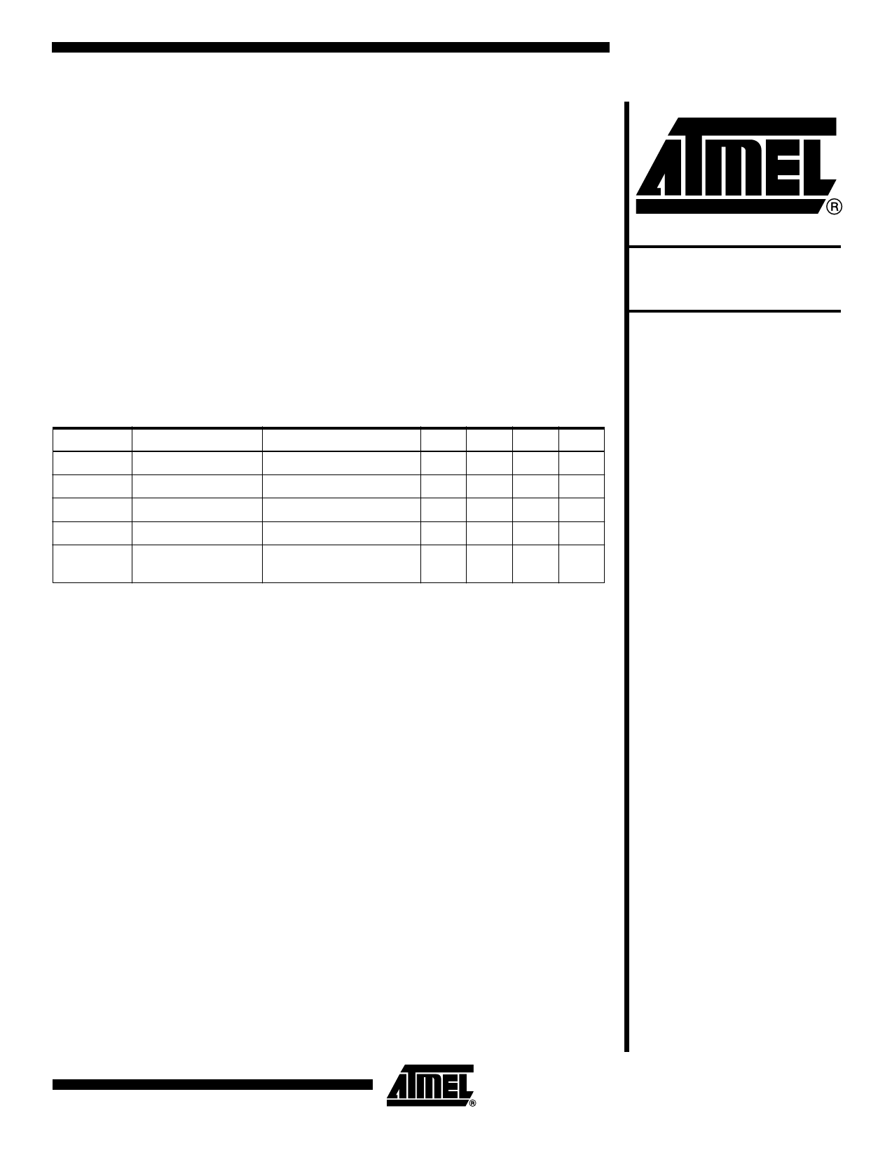
Table 1. Recommended Operating Conditions
Symbol
Parameter
Conditions
VDD
VDD3
VI
VO
TEMP
DC Supply Voltage
DC Supply Voltage
DC Input Voltage
DC Output Voltage
Operating Free Air
Temperature Range
Core and Standard I/Os
3V Interface I/Os
Industrial
Min Typ Max Unit
2.25 2.5 2.75
V
3
3.3 3.6
V
0
VDD
V
0
VDD
V
-40
+85
°C
The Atmel cell libraries and megacell compilers have been designed in order to be
compatible with each other. Simulation representations exist for three types of operat-
ing conditions; they correspond to three characterization conditions defined as follows:
• MIN conditions:
TJ = -40°C
VDD (cell) = 2.75V
Process = fast (industrial best case)
• TYP conditions:
TJ = +25°C
VDD (cell) = 2.5V
Process = typ (industrial typical case)
• MAX conditions:
TJ = +100°C
VDD (cell) = 2.25V
Process = slow (industrial worst case)
Delays to tri-state are defined as delay to turn off (VGS < VT) of the driving devices.
Output pad drain current corresponds to the output current of the pad when the output
voltage is VOL or VOH. The output resistor of the pad and the voltage drop due to
access resistors (in and out of the die) are taken into account. In order to have accu-
rate timing estimates, all characterization has been run on electrical netlists extracted
from the layout database.
Cell-based ASIC
ATC25
Summary
Rev. 1306DS–CBIC–09/02
1
Share Link: 