ATT3042 데이터 시트보기 (PDF) - Unspecified
부품명
상세내역
제조사
ATT3042 Datasheet PDF : 80 Pages
| |||
Data Sheet
February 1997
ATT3000 Series Field-Programmable Gate Arrays
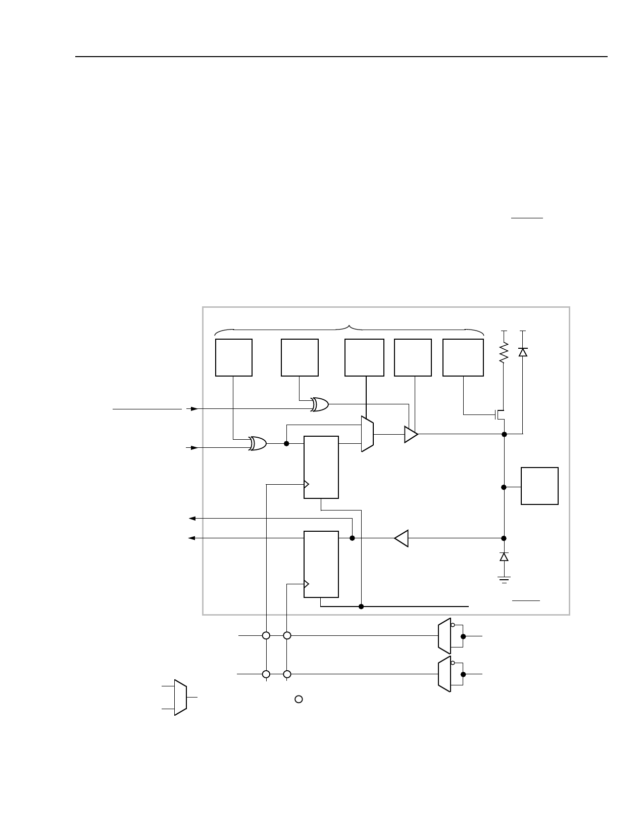
I/O Block
Each user-configurable I/O block (IOB), shown in
Figure 3, provides an interface between the external
package pin of the device and the internal user logic.
Each IOB includes both registered and direct input
paths and a programmable 3-state output buffer which
may be driven by a registered or direct output signal.
Configuration options allow each IOB an inversion, a
controlled slew rate, and a high-impedance pull-up.
Each input circuit also provides input clamping diodes
to provide electrostatic protection and circuits to inhibit
latch-up produced by input currents.
The input buffer portion of each IOB provides threshold
detection to translate external signals applied to the
package pin to internal logic levels. The global input-
buffer threshold of the IOB can be programmed to be
compatible with either TTL or CMOS levels. The buff-
ered input signal drives the data input of a storage
element which may be configured as a positive-edge
triggered D flip-flop or a low-level transparent latch. The
sense of the clock can be inverted (negative edge/high
transparent) as long as all IOBs on the same clock net
use the same clock sense. Clock/load signals (IOB pins
.ik and .ok) can be selected from either of two die edge
metal lines. I/O storage elements are reset during con-
figuration or by the active-low chip RESET input. Both
direct input (from IOB pin .i) and registered input (from
IOB pin .q) signals are available for interconnect.
PROGRAM-CONTROLLED MEMORY CELLS
VCC
OUT
INVERT
3-STATE
INVERT
OUTPUT
SELECT
SLEW
RATE
PASSIVE
PULL UP
3-STATE
.t
OUTPUT ENABLE
.o
OUT
.i
DIRECT IN
REGISTERED IN
.q
DQ
FLIP-
FLOP
R
OUTPUT
BUFFER
I/O PAD
QD
FLIP-
FLOP
OR
LATCH
R
TTL OR
CMOS
INPUT
THRESHOLD
.ok
.lk
(GLOBAL RESET)
CK1
PROGRAM-
CONTROLLED
MULTIPLEXER
CK2
= PROGRAMMABLE INTERCONNECTION POINT OR PIP
Figure 3. Input/Output Block
5-3102(F)
Lucent Technologies Inc.
5
Share Link: 