PI74FCT162646T 데이터 시트보기 (PDF) - Pericom Semiconductor
부품명
상세내역
제조사
PI74FCT162646T Datasheet PDF : 8 Pages
| |||
PI74FCT16646T/162646T/162H646T
11223344556677889900112233445566778899001122334455667788990011221122334455667788990011223344556677889900112233445566778899001122112233445566778899001122334455667788990011223344556677889900112211223314465566-77B8899i00t11R223344e55g6677i88s99t00e11r2233e44d5566T778899r00a1122n11s22c3344e55i66v7788e99r00s1122
Truth Table
Inputs
DATA I/O(2)
Function/Operation
xOE
XDIR XCLKAB XCLKBA XSAB XSBA
XAX
XBX
Isolation
Store A and B Data
H
X
H or L
H or L
X
X
Input
Input
H
X
↑
↑
X
X
Real Time B Data to A Bus
Stored B Data to A Bus
L
L
X
X
X
L
Output
Input
L
L
X
H or L
X
H
Real Time A Data to B Bus
Stored A Data to B Bus
L
H
X
X
L
X
Input
Output
L
H
H or L
X
H
X
Notes:
1.The data output functions may be enabled or disabled by various signals at the xOE or xDIR inputs.
Data input functions are always enabled, i.e., data at the bus pins will be stored on every low-to-high transition on the clock inputs.
2. Select control = L: clocks can occur simultaneously.
Select control = H: clocks must be staggered to load both registers.
H = High Voltage Level; L = Low Voltage Level; X = Don’t Care; ↑ = LOW-to-HIGH transition
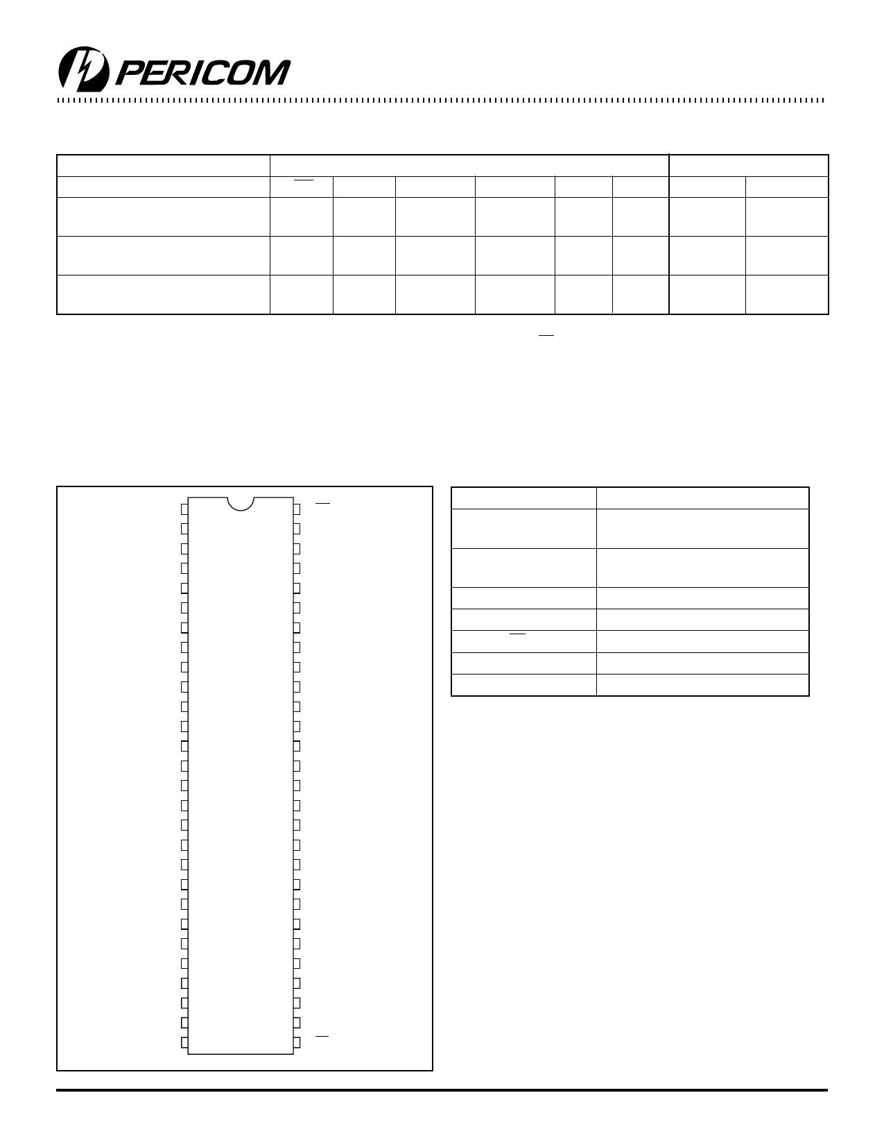
Product Pin Configuration
1DIR
1CLKAB
1SAB
GND
1A0
1A1
VCC
1A2
1A3
1A4
GND
1A5
1A6
1A7
2A0
2A1
2A2
GND
2A3
2A4
2A5
VCC
2A6
2A7
GND
2SAB
2CLKAB
2DIR
1
56
2
55
3
54
4
53
5
52
6
51
7
50
8
49
9
48
10 56-PIN 47
V56
11 A56 46
12 K56 45
13
44
14
43
15
42
16
41
17
40
18
39
19
38
20
37
21
36
22
35
23
34
24
33
25
32
26
31
27
30
28
29
1OE
1CLKBA
1SBA
GND
1B0
1B1
VCC
1B2
1B3
1B4
GND
1B5
1B6
1B7
2B0
2B1
2B2
GND
2B3
2B4
2B5
VCC
2B6
2B7
GND
2SBA
2CLKBA
2OE
Product Pin Description
Pin Name
xAx(1)
xBx(1)
xCLKAB, xCLKBA
SAB, SBA
xDIR, xOE
GND
VCC
Description
Data Register A Inputs
Data Register B Outputs
Data Register B Inputs
Data Register A Outputs
Clock Pulse Inputs
Output Data Source Select Inputs
Output Enable Inputs
Ground
Power
Note: 1.For the PI74FCT162H646T, these pins have
“Bus Hold.” All other pins are standard, outputs, or I/Os.
2
PS2039B 02/24/99
Share Link: 