PI74FCT162646T 데이터 시트보기 (PDF) - Pericom Semiconductor
부품명
상세내역
제조사
PI74FCT162646T Datasheet PDF : 8 Pages
| |||
PI74FCT16646T/162646T/162H646T
11223344556677889900112233445566778899001122334455667788990011221122334455667788990011223344556677889900112233445566778899001122112233445566778899001122334455667788990011223344556677889900112211223314465566-77B8899i00t11R223344e55g6677i88s99t00e11r2233e44d5566T778899r00a1122n11s22c3344e55i66v7788e99r00s1122
Maximum Ratings
(Above which the useful life may be impaired. For user guidelines, not tested.)
Storage Temperature ................................................................. –65°C to +150°C
Ambient Temperature with Power Applied ................................ –40°C to +85°C
Supply Voltage to Ground Potential (Inputs & Vcc Only) .......... –0.5V to +7.0V
Supply Voltage to Ground Potential (Outputs & D/O Only) ....... –0.5V to +7.0V
DC Input Voltage ......................................................................... –0.5V to +7.0V
DC Output Current .................................................................................... 120mA
Power Dissipation ......................................................................................... 1.0W
Note:
Stresses greater than those listed under
MAXIMUM RATINGS may cause permanent
damage to the device. This is a stress rating only
and functional operation of the device at these
or any other conditions above those indicated in
the operational sections of this specification is
not implied. Exposure to absolute maximum
rating conditions for extended periods may
affect reliability.
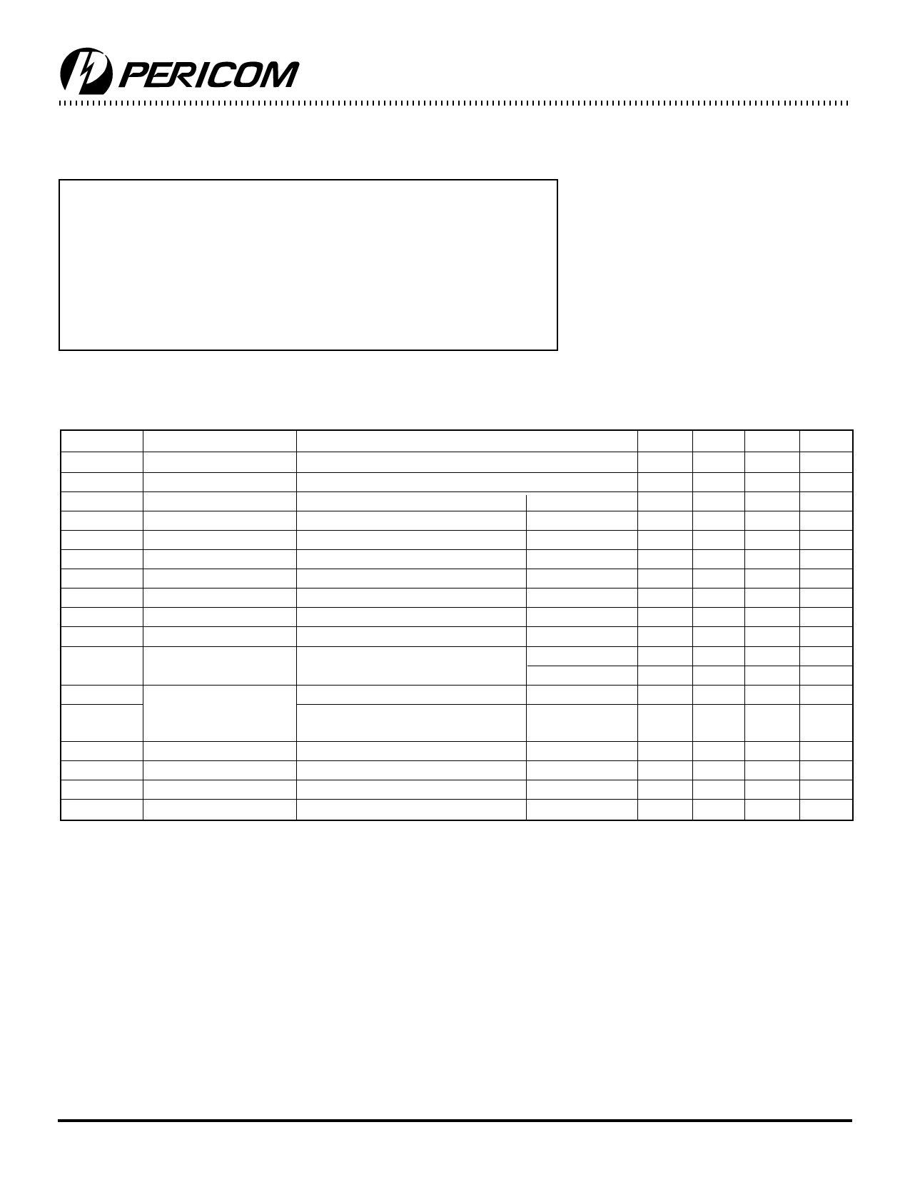
DC Electrical Characteristics (Over the Operating Range, TA = 40°C to +85°C, VCC = 5.0V ± 10%)
Parameters Description
Test Conditions(1)
Min. Typ.(2)
VIH
VIL
IIH
IIH
IIH
IIH
IIL
IIL
IIL
IIL
IBHH
IBHL
IOZH(5)
IOZL(5)
VIK
IOS
IO
VH
Input HIGH Voltage
Input LOW Voltage
Input HIGH Current
Input HIGH Current
Input HIGH Current
Input HIGH Current
Input LOW Current
Input LOW Current
Input LOW Current
Input LOW Current
Bus Hold
Sustain Current
High-Impedance
Output Current
(3-STATE OUTPUTS)
Clamp Diode Voltage
Short Circuit Current
Output Drive Current
Input Hysteresis
Guaranteed Logic HIGH Level
Guaranteed Logic LOW Level
Standard Input, VCC = Max.
Standard I/O, VCC = Max.
Bus Hold Input(4), VCC = Max.
Bus Hold I/O(4), VCC = Max.
Standard Input, VCC = Min.
Standard I/O, VCC = Min.
Bus Hold Input(4), VCC = Min.
Bus Hold I/O(4), VCC = Min.
Bus Hold Input(4), VCC = Min.
VCC = Max.
VCC = Max.
VCC = Min., IIN = 18mA
VCC = Max.(3), VOUT = GND
VCC = Max.(3), VOUT = 2.5V
VIN = VCC
VIN = VCC
VIN = VCC
VIN = VCC
VIN = GND
VIN = GND
VIN = GND
VIN = GND
VIN = 2.0V
VIN = 0.8V
VOUT = 2.7V
VOUT = 0.5V
2.0
50
+50
0.7
80 140
50
100
Max.
0.8
1
1
±100
±100
1
1
±100
±100
1
1
1.2
200
180
Units
V
V
µA
µA
µA
µA
µA
µA
µA
µA
µA
µA
µA
V
mA
mA
mV
Notes:
1. For Max. or Min. conditions, use appropriate value specified under Electrical Characteristics for the applicable device type.
2. Typical values are at Vcc = 5.0V, +25°C ambient and maximum loading.
3. Not more than one output should be shorted at one time. Duration of the test should not exceed one second.
4. Pins with Bus Hold are identified in the pin description.
5. This specification does not apply to bi-directional functionalities with Bus Hold.
4
PS2039B 02/24/99
Share Link: 