BCR20AM 데이터 시트보기 (PDF) - Powerex
부품명
상세내역
제조사
BCR20AM Datasheet PDF : 4 Pages
| |||
Powerex, Inc., 200 Hillis Street, Youngwood, Pennsylvania 15697-1800 (412) 925-7272
BCR20AM
Triac
20 Ampere/400-600 Volts
Absolute Maximum Ratings, Ta = 25 °C unless otherwise specified
Ratings
Symbol
On-state Current, Tc = 105°C
Repetitive Peak Off-state Voltage (Gate Open)
Non-repetitive Peak Off-state Voltage (Gate Open)
Non-repetitive Peak On-state Voltage, One Cycle (60 Hz)
I2t for Fusing, t = 8.3 msec
IT(RMS)
VDRM
VDSM
ITSM
I2t
Peak Gate Power Dissipation, 20 sec
Average Gate Power Dissipation
Peak Gate Current
Peak Gate Voltage
Storage Temperature
Operating Temperature
Weight
PGM
PG(avg)
IGM
VGM
Tstg
Tj
–
BCR20AM-8
20
400
500
200
167
5
0.5
2
10
-40 to 125
-40 to 125
2.0
BCR20AM-12
20
600
720
200
167
5
0.5
2
10
-40 to 125
-40 to 125
2.0
Units
Amperes
Volts
Volts
Amperes
A2sec
Watts
Watts
Amperes
Volts
°C
°C
Grams
Electrical and Thermal Characteristics, Tj = 25 °C unless otherwise specified
Test Conditions (Trigger Mode)
Characteristics
Symbol
VD
RL
RG
Tj
Gate Parameters
DC Gate Trigger Current
MT2+ Gate+
MT2+ Gate–
MT2– Gate–
DC Gate Trigger Voltage
IFGT I
IRGT I
IRGT III
6V
6⍀
330⍀ 25°C
6V
6⍀
330⍀ 25°C
6V
6⍀
330⍀ 25°C
MT2+ Gate+
MT2+ Gate–
MT2– Gate–
DC Gate Non-trigger Voltage
VFGT I
VRGT I
VRGT III
6V
6⍀
330⍀ 25°C
6V
6⍀
330⍀ 25°C
6V
6⍀
330⍀ 25°C
All
VGD
1/2 VDRM –
–
125°C
Thermal Resistance, Junction-to-case
Voltage – Blocking State
Repetitive Off-state Current
Current – Conducting State
Peak On-state Voltage
Critical Rate-of-Rise of Commutating
Off-state Voltage (Commutating dv/dt)
v (Switching)
Rth(j-c)
IDRM
VTM
(dv/dt)c
–
Gate Open Circuited,
VD = VDRM, Tj = 125°C
Tc = 25°C,
ITM = 30A
–
BCR30GM
Min.
Typ. Max.
Units
–
–
–
–
–
–
–
–
–
–
–
–
0.2
–
–
–
–
–
–
–
–
–
30
mA
30
mA
30
mA
1.5 Volts
1.5 Volts
1.5 Volts
–
Volts
0.8 °C/W
2
mA
1.5 Volts
–
V/s
⌬ Part
Number
VDRM
(Volts)
BCR20AM-8 400
BCR20AM-8L
BCR20AM-12 600
BCR20AM-12L
T-84
Commutating dv/dt,
(dv/dt)c (V/sec) Minimum
—
10
—
10
Test Condition
Tj = 125°C, Rate of Decay
On-state Commutating Current
(dv/dt)c = -10A/msec,
Peak Off-state Voltage VD = 400V
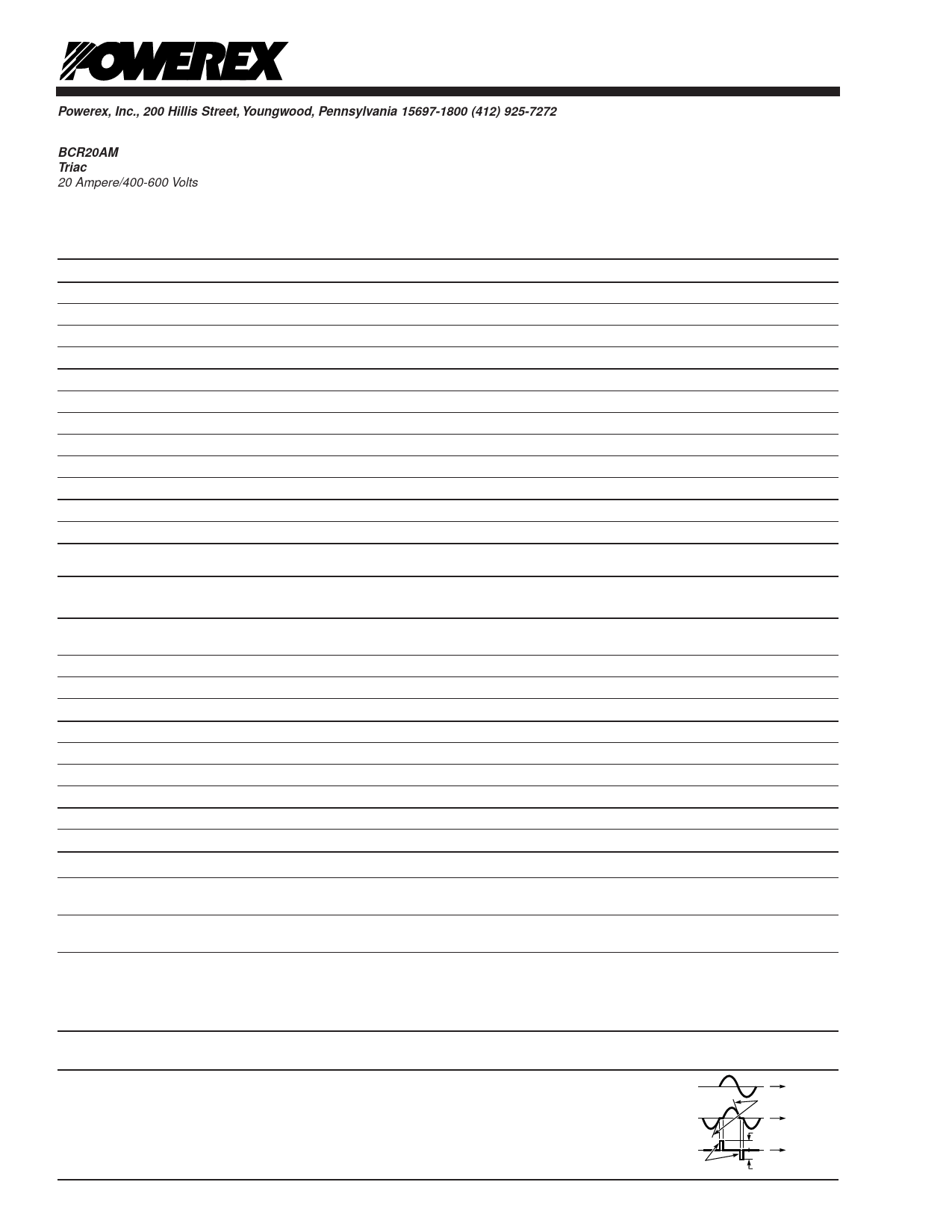
Commutating Voltage & Current Waveform
(Inductive Load)
SUPPLY
VOLTAGE
MAIN
CURRENT
t
(di/dt)C
t
MAIN
VOLTAGE
(dv/dt)C
VD
t
VD
Share Link: 