Q62702-F1372 데이터 시트보기 (PDF) - Siemens AG
부품명
상세내역
제조사
Q62702-F1372 Datasheet PDF : 5 Pages
| |||
BF 543
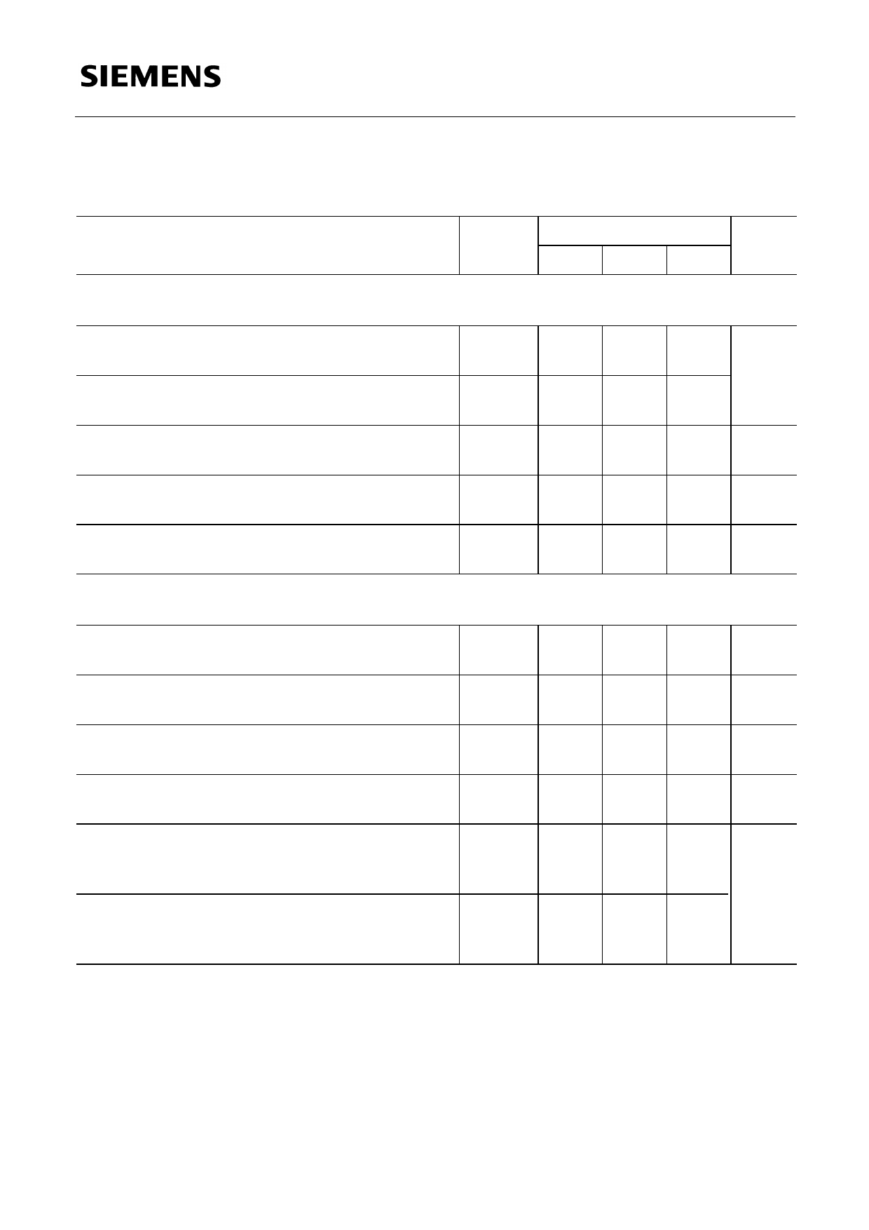
Electrical Characteristics
at TA = 25 ˚C, unless otherwise specified.
Parameter
DC Characteristics
Drain-source breakdown voltage
ID = 10 µA, – VGS = 4 V
Gate-source breakdown voltage
± IGS = 10 mA, VDS = 0
Gate cutoff current
± VGS = 6 V, VDS = 0
Drain current
VDS = 10 V, VGS = 0
Gate-source pinch-off voltage
VDS = 10 V, ID = 20 µA
AC Characteristics
Forward transconductance
VDS = 10 V, ID = 4 mA, f = 1 kHz
Gate-1 input capacitance
VDS = 10 V, ID = 4 mA, f = 1 MHz
Reverse transfer capacitance
VDS = 10 V, ID = 4 mA, f = 1 MHz
Output capacitance
VDS = 10 V, ID = 4 mA, f = 1 MHz
Power gain (test circuit)
VDS = 10 V, ID = 4 mA, f = 200 MHz
GG = 2 mS, GL = 0.5 mS
Noise figure (test circuit)
VDS = 10 V, ID = 4 mA, f = 200 MHz
GG = 2 mS, GL = 0.5 mS
Symbol
Values
Unit
min. typ. max.
V(BR)DS
20
–
–
V
V ± (BR)GSS 7
–
12
± IGSS
–
–
50 nA
IDSS
2.0 4
6.0 mA
– VGS(p) –
0.7 1.5 V
gfs
9.5 12 –
mS
Cgss
–
2.7 –
pF
Cdg
–
18 –
fF
Cdss
–
0.9 –
pF
Gp
–
22 –
dB
F
–
1
–
Semiconductor Group
2
Share Link: 