CM900HB-90H 데이터 시트보기 (PDF) - MITSUBISHI ELECTRIC
부품명
상세내역
제조사
CM900HB-90H Datasheet PDF : 4 Pages
| |||
2nd-Version HVIGBT (High Voltage Insulated Gate Bipolar Transistor) Modules
MITSUBISHI HVIGBT MODULES
CM900HB-90H
HIGH POWER SWITCHING USE
INSULATED TYPE
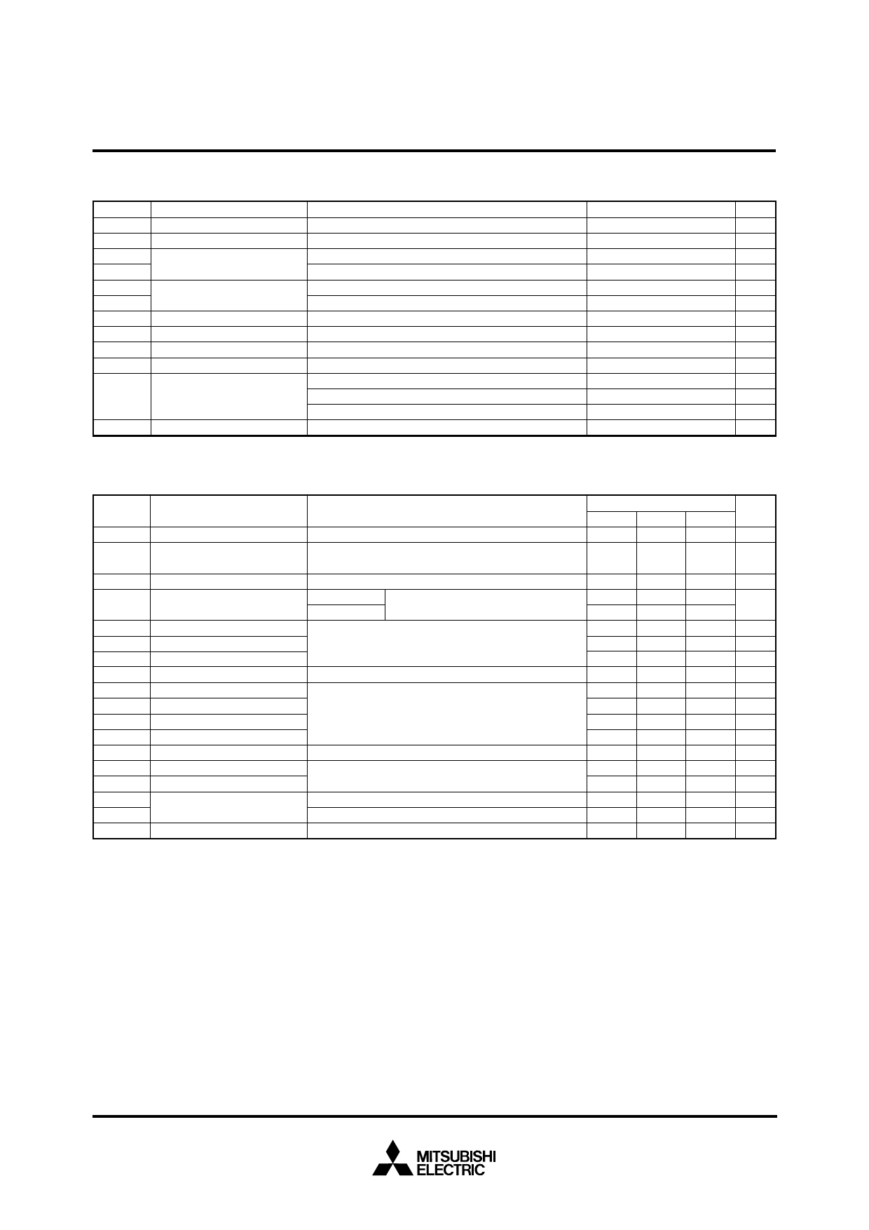
MAXIMUM RATINGS (Tj = 25°C)
Symbol
Item
Conditions
Ratings
Unit
VCES
Collector-emitter voltage
VGE = 0V
4500
V
VGES
Gate-emitter voltage
VCE = 0V
±20
V
IC
Collector current
ICM
DC, TC = 85°C
Pulse
900
A
(Note 1)
1800
A
IE (Note 2) Emitter current
IEM(Note 2)
Pulse
900
A
(Note 1)
1800
A
PC (Note 3) Maximum collector dissipation TC = 25°C, IGBT part
11100
W
Tj
Junction temperature
—
–40 ~ +125
°C
Tstg
Storage temperature
—
–40 ~ +125
°C
Viso
Isolation voltage
Charged part to base plate, rms, sinusoidal, AC 60Hz 1min.
6000
V
Main terminals screw M8
6.67 ~ 13.00
N·m
—
Mounting torque
Mounting screw M6
2.84 ~ 6.00
N·m
Auxiliary terminals screw M4
0.88 ~ 2.00
N·m
—
Mass
Typical value
2.2
kg
ELECTRICAL CHARACTERISTICS (Tj = 25°C)
Symbol
Item
Conditions
Min
ICES
Collector cutoff current
VCE = VCES, VGE = 0V
—
Gate-emitter
VGE(th)
threshold voltage
IC = 90mA, VCE = 10V
4.5
IGES
Gate-leakage current
VGE = VGES, VCE = 0V
—
VCE(sat)
Collector-emitter
saturation voltage
Tj = 25°C
Tj = 125°C
IC = 900A, VGE = 15V
—
(Note 4) —
Cies
Input capacitance
VCE = 10V
—
Coes
Output capacitance
VGE = 0V
—
Cres
Reverse transfer capacitance
—
QG
Total gate charge
VCC = 2250V, IC = 900A, VGE = 15V
—
td (on)
Turn-on delay time
VCC = 2250V, IC = 900A
—
tr
Turn-on rise time
VGE1 = VGE2 = 15V
—
td (off)
Turn-off delay time
RG = 10Ω
—
tf
Turn-off fall time
Resistive load switching operation
—
VEC(Note 2)
trr (Note 2)
Qrr (Note 2)
Rth(j-c)Q
Rth(j-c)R
Rth(c-f)
Emitter-collector voltage
Reverse recovery time
Reverse recovery charge
Thermal resistance
Contact thermal resistance
IE = 900A, VGE = 0V
IE = 900A,
die / dt = –1800A / µs
Junction to case, IGBT part
Junction to case, FWDi part
Case to fin, conductive grease applied
—
—
(Note 1) —
—
—
—
Note 1. Pulse width and repetition rate should be such that the device junction temp. (Tj) does not exceed Tjmax rating.
2. IE, VEC, trr, Qrr & die/dt represent characteristics of the anti-parallel, emitter to collector free-wheel diode.
3. Junction temperature (Tj) should not increase beyond 125°C.
4. Pulse width and repetition rate should be such as to cause negligible temperature rise.
Limits
Typ
—
Unit
Max
18 mA
6.0
7.5 V
—
0.5 µA
3.00 3.90
3.30
—
V
162
—
nF
12.0
—
nF
3.6
—
nF
—
—
µC
—
2.40 µs
—
2.40 µs
—
6.00 µs
—
1.20 µs
4.00 5.20 V
—
1.80 µs
360
—
µC
—
0.009 K/W
—
0.018 K/W
0.007
—
K/W
HVIGBT MODULES (High Voltage Insulated Gate Bipolar Transistor Modules)
Mar. 2003
Share Link: 