CS52015-1 데이터 시트보기 (PDF) - ON Semiconductor
부품명
상세내역
제조사
CS52015-1 Datasheet PDF : 9 Pages
| |||
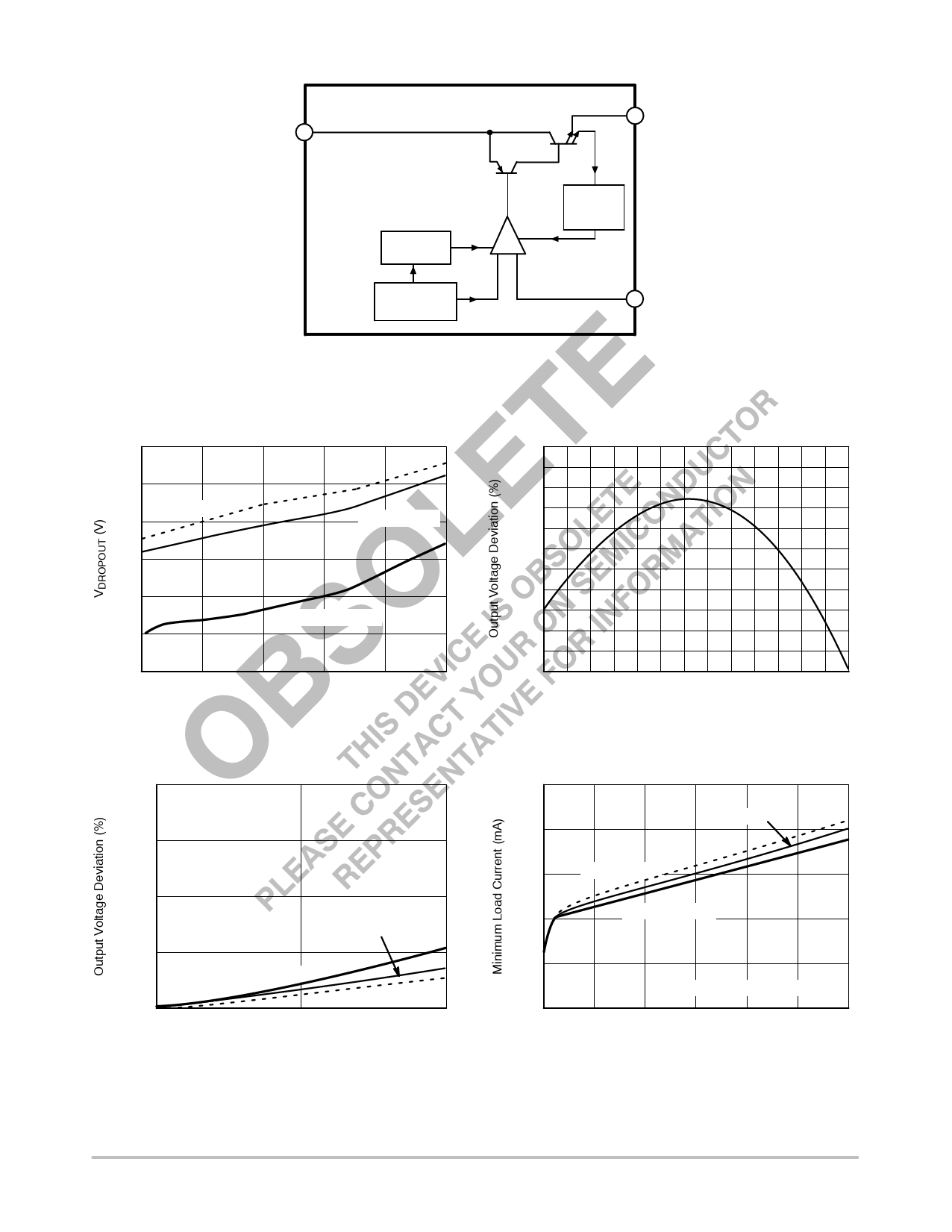
CS52015−1
VOUT
VIN
Thermal
Shutdown
Bandgap
Output
Current
Limit
− + Error
Amplifier
Adj
Figure 2. Block Diagram
TYPICAL PERFORMANCE CHARACTERISTICS
1.05
1.00
0.95
TCASE = 0°C
TCASE = 25°C
0.90
0.85
0.80
TCASE = 125°C
0.75
0
300
600
900
1200
IOUT (mA)
Figure 3. Dropout Voltage vs. Output
Current
1500
0.10
0.08
0.06
0.04
0.02
0.00
−0.02
−0.04
−0.06
−0.08
−0.10
−0.12
0
10 20 30
40 50 60 70 80 90 100 110 120 130
TJ (°C)
Figure 4. Reference Voltage vs.
Temperature
0.100
0.075
0.050
0.025
TCASE = 25°C
TCASE = 125°C
0.000
0
1
Output Current (A)
TCASE = 0°C
2
Figure 5. Load Regulation vs. Output
Current
0.65
0.60
0.55
0.50
TCASE = 25°C
TCASE = 0°C
TCASE = 125°C
0.45
0.40
1
CIN = COUT = 22 mF Tantalum
2
3
4
5
6
7
VIN − VOUT (V)
Figure 6. Minimum Load Current vs.
VIN − VOUT
http://onsemi.com
3
Share Link: 