CXB1582Q 데이터 시트보기 (PDF) - Sony Semiconductor
부품명
상세내역
제조사
CXB1582Q Datasheet PDF : 23 Pages
| |||
Pin
No.
Symbol
25, 42,
62, 76, VCCG
77
Type
Typical pin
I/O voltage
Power
supply
3.3V
26, 41,
61, 75
VEEG
Power
supply
0V
33 RBC0
TTL
output
TTL level
34 RBC1
TTL
output
TTL level
35 SYNC
TTL
output
TTL level
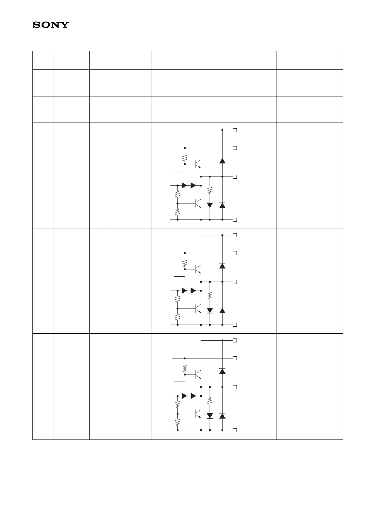
CXB1582Q
Equivalent circuit
—
—
VCCT5
VCCT3
RBC0
VEET
VCCT5
VCCT3
RBC1
Description
Positive power
supplies for internal
logic gate.
Negative power
supplies for internal
logic gate.
Receive byte clock 0
output.
This clock is used
when loading parallel
data (RX00 to RX19)
using the system in
the next stage.
Receive byte clock 1
output.
Inverse of the RBC0
clock.
VEET
VCCT5
VCCT3
SYNC
VEET
Byte sync output.
This pin outputs high
level when
+Comma (0011111)
or
–Comma (1100000)
is detected in the
serial data. (See the
Timing Charts.)
–5–
Share Link: 