EL4344C 데이터 시트보기 (PDF) - Elantec -> Intersil
부품명
상세내역
제조사
EL4344C Datasheet PDF : 10 Pages
| |||
EL4331
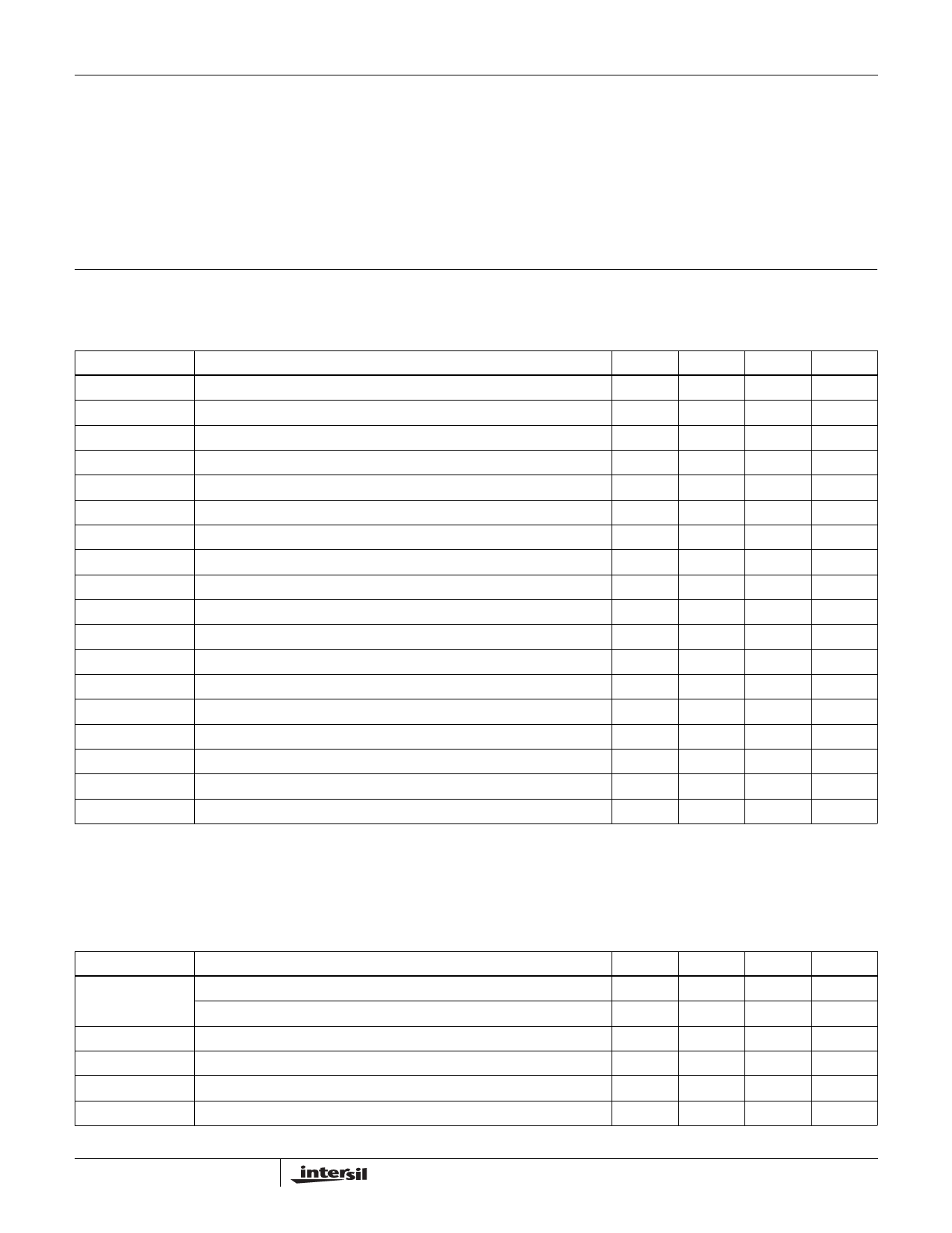
Absolute Maximum Ratings (TA = 25°C)
VCC to VEE . . . . . . . . . . . . . . . . . . . . . . . . . . . . . . . . . . . . . . . . .14V
VCC to Any GND . . . . . . . . . . . . . . . . . . . . . . . . . . . . . . . . . . . . .12V
VEE to Any GND . . . . . . . . . . . . . . . . . . . . . . . . . . . . . . . . . . . . .12V
Continuous Output Current . . . . . . . . . . . . . . . . . . . . . . . . . . . 45mA
Any Input (except PD) . . . . . . . . . . . . . . . . . VEE-0.3V to VCC+0.3V
PD Input . . . . . . . . . . . . . . . . . . . . . . . . . . . . . .VCC-7V to VCC+0.3V
Input Current, Any Input. . . . . . . . . . . . . . . . . . . . . . . . . . . . . . . 5mA
Power Dissipation . . . . . . . . . . . . . . . . . . . . . . . . . . . . . . See curves
Ambient Operating Temperature . . . . . . . . . . . . . . . .-40°C to +85°C
Junction Temperature . . . . . . . . . . . . . . . . . . . . . . . . . . . . . . . 150°C
Storage Temperature . . . . . . . . . . . . . . . . . . . . . . . .-65°C to +150°C
CAUTION: Stresses above those listed in “Absolute Maximum Ratings” may cause permanent damage to the device. This is a stress only rating and operation of the
device at these or any other conditions above those indicated in the operational sections of this specification is not implied.
IMPORTANT NOTE: All parameters having Min/Max specifications are guaranteed. Typical values are for information purposes only. Unless otherwise noted, all tests
are at the specified temperature and are pulsed tests, therefore: TJ = TC = TA
DC Electrical Specifications VCC = +5V, VEE = -5V, Ambient Temperature = 25°C, RL = 500Ω, PD = 5V
PARAMETER
DESCRIPTION
MIN
TYP
VOS
dVOS
IB
dIB
AVOL
PSRR
Input Referred Offset Voltage
Input A to Input B Offset Voltage (Note 1)
Input Bias Current
Input A to Input B Bias Current (Note 1)
Open Loop Gain (from Gain Error Calculation)
Power Supply Rejection Ratio
-12
1
-7
0.5
54
60
70
VOUT_500
VOUT_150
IOUT
XTALK
VIH
VIL
IIL_AB
IIH_AB
IIL_PD
IIH_PD
IS
IS(PD)
Output Voltage Swing into 500Ω Load
Output Voltage Swing into 150Ω Load
Current Output, Measured with 75Ω load (Note 2)
Crosstalk from Non-Selected Input (at DC)
Input Logic High Level (A/B and PD)
Input Logic Low Level (A/B and PD)
Logic Low Input Current (VIN = 0.8V), A/B Pin
Logic High Input Current (VIN = 2.0V), A/B Pin
Logic Low Input Current (VIN = 0.8V), PD Pin
Logic High Input Current (VIN = 5.0V), PD Pin
Total Supply Current
Powered Down Supply Current
±2.7
±3.2
+3/-2.7
30
40
-70
-85
2.0
-1
-20
-5
0
-10
0
0.5
1.0
38
48
0.01
NOTES:
1. Any channel’s A-input to its B-input.
2. There is no short circuit protection on any output.
MAX
30
8
-30
4.0
0.8
-100
5
10
1.6
60
1.0
UNIT
mV
mV
µA
µA
dB
dB
V
V
mA
dB
V
V
µA
µA
µA
mA
mA
mA
AC Electrical Specifications VCC = +5V, VEE = -0.5V, Ambient Temperature = 25°C, RL = 150Ω and CL = 5pF
PARAMETER
DESCRIPTION
MIN
TYP
BW
-3dB Bandwidth
300
-3dB BW with 250Ω and 10pF Load
400
SR
Slew Rate (4V Square Wave, Measured 25%–75%)
400
TS
Settling Time to 0.1% of Final Value
13
TAB
Time to Switch Inputs
3
OS
Overshoot, VOUT = 4Vpk-pk
8
MAX
UNIT
MHz
MHz
V/µs
ns
ns
%
2
Share Link: 