LC662104A 데이터 시트보기 (PDF) - SANYO -> Panasonic
부품명
상세내역
제조사
LC662104A Datasheet PDF : 13 Pages
| |||
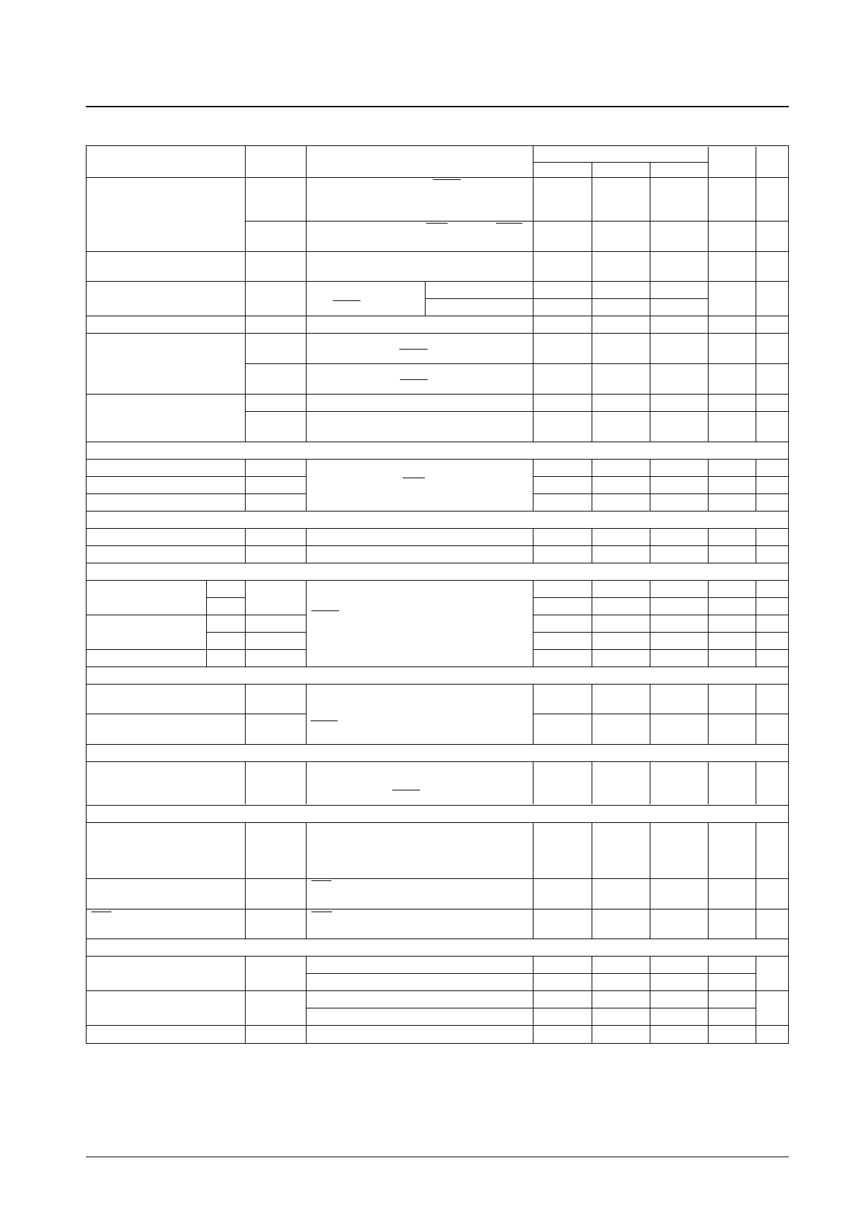
LC662104A, 662106A, 662108A
Electrical Characteristics at Ta = –30 to +70°C, VSS = 0 V, VDD = 3.0 to 5.5 V unless otherwise specified.
Parameter
Input high-level current
Input low-level current
Output high-level voltage
Value of the output pull-up resistor
Output low-level voltage
Output off leakage current
[Schmitt characteristics]
Hysteresis voltage
High-level threshold voltage
Low-level threshold voltage
[Ceramic oscillator]
Oscillator frequency
Oscillator stabilization time
[Serial clock]
Cycle time
Input
Output
Low-level and high-level Input
pulse widths
Output
Rise an fall times
Output
[Serial input]
Symbol
IIH1
IIH2
IIL1
VOH1
RPO
VOL1
VOL2
IOFF1
IOFF2
VHYS
VtH
VtL
fCF
fCFS
tCKCY
tCKL
tCKH
tCKR, tCKF
Conditions
P2, P3 (except for the P33/HOLD pin), P4,
P51, and P53: VIN = 13.5 V, with the output
Nch transistor off
P0, P1, P50, P52, OSC1, RES, and P33/HOLD:
VIN = VDD, with the output Nch transistor off
P0, P1, P2, P3, P4, and P5:
VIN = VSS, with the output Nch transistor off
P2, P3 (except for the IOH = –1 mA
P33/HOLD pin)
IOH = –0.1 mA
P0, P1, P4, P5
P0, P1, P2, P3, P4, and P5
(except for the P33/HOLD pin): IOL = 1.6 mA
P0, P1, P2, P3, P4, and P5
(except for the P33/HOLD pin): IOL = 8 mA
P2, P3, P4, P51, and P53: VIN = 13.5 V
Does not apply to P2, P3, P4, P51, and P53:
VIN = VDD
P2, P3, P4, P5, and RES
OSC1, OSC2: See Figure 2. 4 MHz
See Figure 3. 4 MHz
SCK0: With the timing of Figure 4 and the test
load of Figure 5.
min
–1.0
VDD – 1.0
VDD – 0.5
30
0.5 VDD
0.2 VDD
0.9
2.0
0.4
1.0
Ratings
typ
100
0.1 VDD
4.0
max
5.0
1.0
150
0.4
1.5
5.0
1.0
0.8 VDD
0.5 VDD
10.0
0.1
Unit Note
µA
1
µA
1
µA
2
V
3
kΩ
V
5
V
µA
6
µA
6
V
V
MHz
ms
µs
Tcyc
µs
Tcyc
µs
Data setup time
Data hold time
[Serial output]
Output delay time
[Pulse conditions]
INT0 high and low-level
High and low-level pulse widths
for interrupt inputs other than INT0
RES high and low-level
pulse widths
tICK
tCKI
tCKO
tIOH, tIOL
tIIH, tIIL
tRSH, tRSL
SI0: With the timing of Figure 4.
Stipulated with respect to the rising edge (↑) of
SCK0.
SO0: With the timing of Figure 4 and the test
load of Figure 5. Stipulated with respect to the
falling edge (↓) of SCK0.
INT0: Figure 6, conditions under which the INT0
interrupt can be accepted, conditions under
which the timer 0 event counter or pulse width
measurement input can be accepted
INT1, INT2: Figure 6, conditions under which
the corresponding interrupt can be accepted
RES: Figure 6, conditions under which reset
can be applied.
0.3
0.3
2
2
3
µs
µs
0.3
µs
Tcyc
Tcyc
Tcyc
Operating current drain
IDD OP
VDD: 4-MHz ceramic oscillator
VDD: 4-MHz external clock
4.5
8.0
mA
8
4.5
8.0
mA
Halt mode current drain
IDDHALT
VDD: 4-MHz ceramic oscillator
VDD: 4-MHz external clock
2.5
5.5
mA
2.5
5.5
mA
Hold mode current drain
IDDHOLD VDD: VDD = 1.8 to 5.5 V
0.01
10
µA
Note: 1. With the output Nch transistor off in shared I/O ports with the open-drain output specifications. These pins cannot be used as input pins if the
CMOS output specifications are selected.
2. With the output Nch transistor off in shared I/O ports with the open-drain output specifications. The rating for the pull-up output specification pins is
stipulated in terms of the output pull-up current IPO. These pins cannot be used as input pins if the CMOS output specifications are selected.
3. With the output Nch transistor off for CMOS output specification pins.
4. With the output Nch transistor off for pull-up output specification pins.
6. With the output Pch transistor off for open-drain output specification pins.
7. Reset state
No. 5996-11/13
Share Link: 