LC662104A 데이터 시트보기 (PDF) - SANYO -> Panasonic
부품명
상세내역
제조사
LC662104A Datasheet PDF : 13 Pages
| |||
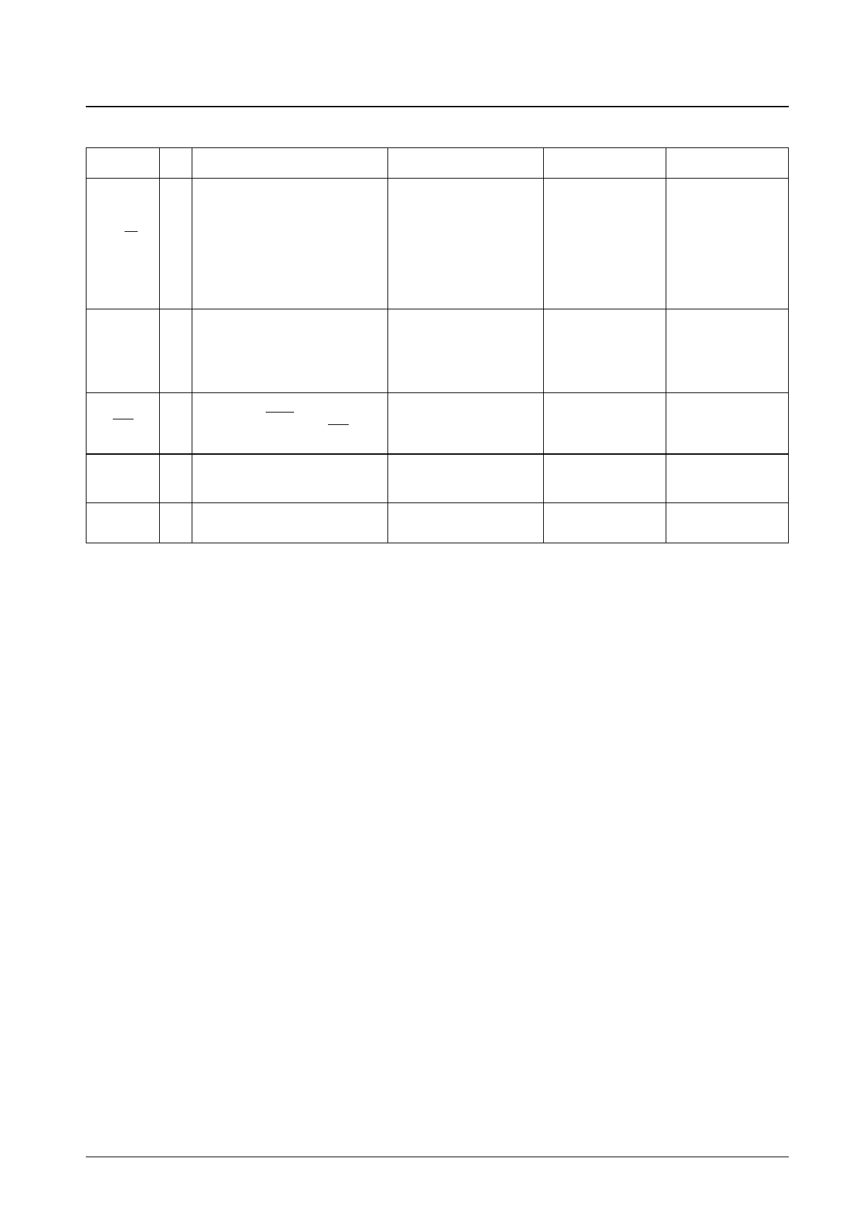
LC662104A, 662106A, 662108A
Continued from preceding page.
Pin
P50
P51/DP
P52/DT
P53/INT2
I/O
Overview
Output driver type
Options
• Pull-up MOS or Nch
I/O
I/O ports P50 to P53
• Input or output in 4-bit or 1-bit units
• P51 is also used for dial pulse output
• P52 is also used for DTMF output
• P53 is also used as the INT2 interrupt
request.
• Pch: Pull-up MOS type
• Nch: Intermediate sink current
type
• Nch: +15-V handling when
OD option selected (P51 and
P53 only)
OD output
• Output level on reset
• Output level after a
reset
(An external pull-up
resistor must be
supplied when used
for DT output.)
State after a
reset
High or low (option)
OSC1
OSC2
I System clock oscillator connections
When an external clock is used, leave
O OSC2 open and connect the clock signal
to OSC1.
RES
System reset input
I
When the P33/HOLD pin is at the high
level, a low level input to the RES pin will
initialize the CPU.
TEST
CPU test pin
I This pin must be connected to VSS
during normal operation.
VDD
VSS
Power supply pins
Note: Pull-up MOS type: The output circuit includes a MOS transistor that pulls the pin up to VDD.
CMOS output: Complementary output.
OD output: Open-drain output.
Ceramic oscillator or
external clock selection
Option selection
No. 5996-6/13
Share Link: 