H5PS2562GFR 데이터 시트보기 (PDF) - Hynix Semiconductor
부품명
상세내역
제조사
H5PS2562GFR Datasheet PDF : 61 Pages
| |||
H5PS2562GFR series
-Continue-
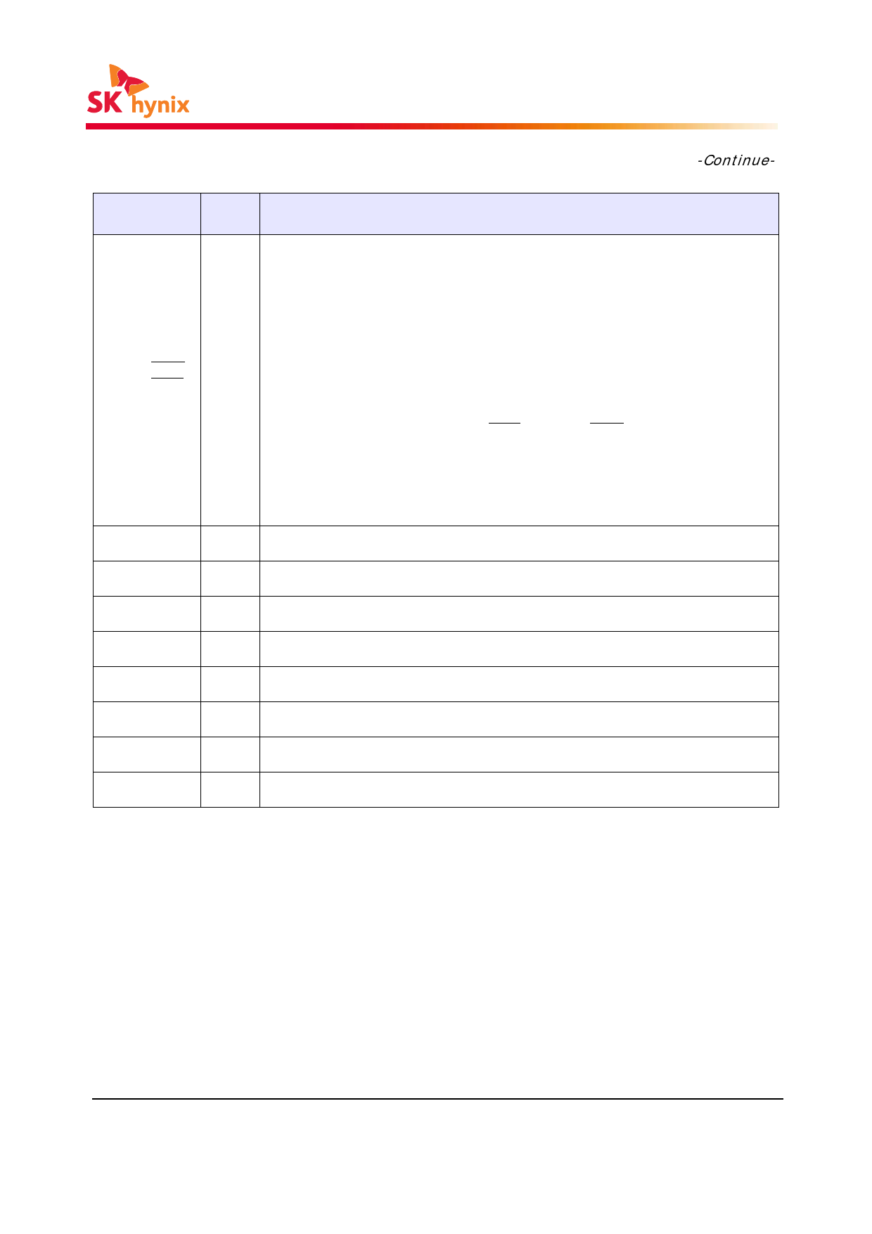
PIN
TYPE
DESCRIPTION
UDQS, UDQS
LDQS, LDQS
Input/
Output
Data Strobe : Output with read data, input with write data. Edge aligned with read data,
centered in write data. For the x16, LDQS correspond to the data on DQ0~DQ7; UDQS
corresponds to the data on DQ8~DQ15. The data strobes DQS, LDQS and UDQS may be
used in single ended mode or paired with optional complementary signals DQS, LDQS
and UDQS to provide differential pair signaling to the system during both reads and
wirtes. An EMRS(1) control bit enables or disables all complementary data strobe sig-
nals.
In this data sheet, "differential DQS signals" refers to any of the following with A10 = 0
of EMRS(1)
of EMRS(1)
x16 LDQS/LDQS and UDQS/UDQS
"single-ended DQS signals" refers to any of the following with A10 = 1
x16 LDQS and UDQS
NC
VDDQ
VSSQ
VDDL
VSSDL
VDD
VSS
VREF
No Connect : No internal electrical connection is present.
Supply DQ Power Supply: 1.8V +/- 0.1V
Supply DQ Ground
Supply DLL Power Supply : 1.8V +/- 0.1V
Supply DLL Ground
Supply Power Supply : 1.8V +/- 0.1V
Supply Ground
Supply Reference voltage for inputs for SSTL interface.
Rev.1.3 / June. 2012
8
Share Link: 