HT8955A 데이터 시트보기 (PDF) - Holtek Semiconductor
부품명
상세내역
제조사
HT8955A Datasheet PDF : 7 Pages
| |||
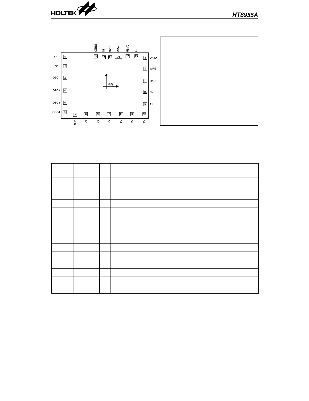
HT8955A
Pad Coordinates
Unit: µm
Pad
No.
X
Y
Pad
No.
X
Y
1 –1138.00 796.50 14 1141.50 –547.00
2 –1141.00 523.50 15 1141.50 –197.50
3 –1136.50 201.50 16 1141.50 111.50
4 –1136.50 –163.00 17 1141.50 461.00
5 –1137.00 –507.00 18 1141.50 770.50
6 –1149.00 –774.00 19 896.00 811.00
7 –854.50 –853.50 20 645.00 810.50
8 –548.00 –831.50 21 435.00 794.00
9 –198.50 –831.50 21 335.00 794.00
10 111.50 –831.50 22 150.00 779.00
11 461.00 –831.50 23 –35.00 779.00
12 773.00 –831.50 25 –264.00 806.00
13 1122.50 –831.50
Chip size: 2170 × 2200 (µm)2
* The IC substrate should be connected to VSS in the PCB layout artwork.
Pin Description
Pin No. Pin Name I/O
Internal
Connection
Description
1
BIAS
O
OP Non-inverted
Internal pre-amplifier bias
Connects to a decoupling capacitor
2
IN
I
OP Inverted Audio signal input pin (inverted)
3
PREO
O OP OUTPUT Pre-amplifier output pin
4
OUT
O
—
Delayed audio signal output pin
5
SEL
DRAM type selection:
I
Pull-High
VDD or Open: 64Kb
VSS: 256Kb
6
OSC1
I
—
System oscillator input
7
OSC2
O
—
System oscillator output
8
OSC3
I
—
Delay time control oscillator input
9
OSC4
O
—
Delay time control oscillator output
10
VSS
I
—
Negative power supply (GND)
11
A6
O
CMOS OUT Connects to DRAM A6
12
A7
O
CMOS OUT Connects to DRAM A7
2
5th May ’98
Share Link: 