LM2931L 데이터 시트보기 (PDF) - HTC Korea
부품명
상세내역
제조사
LM2931L Datasheet PDF : 2 Pages
| |||
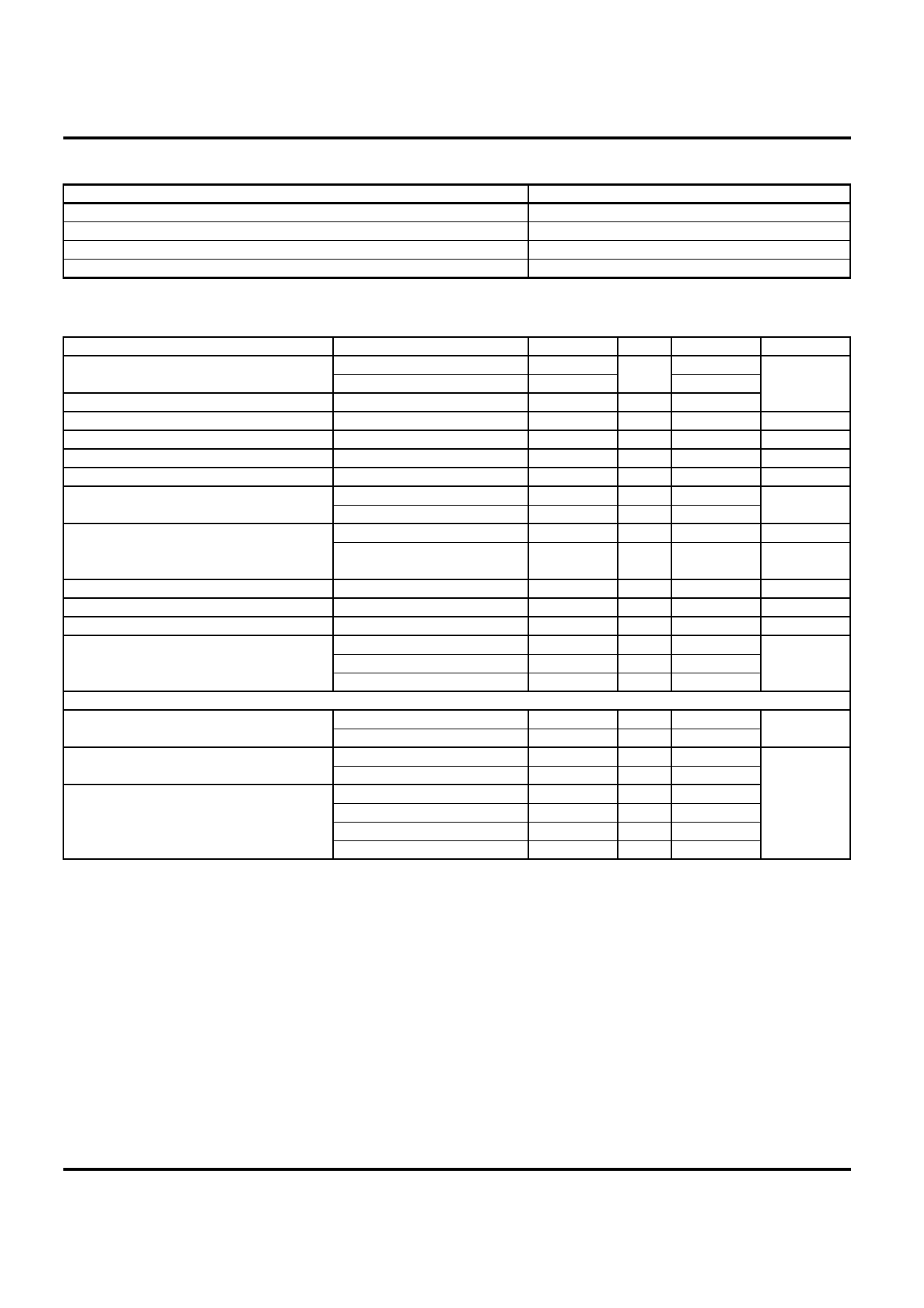
0.1A LOW DROPOUT VOLTAGE REGULATORS
LM2931
ABSOLUTE MAXIMUM RATINGS
POWER DISSIPATION
Lead Temperature (Soldering, 5 seconds)
Storage Temperature Range
Operating Junction Temperature Range
Input Supply Voltage
INTERNALLY LIMITED
260℃
-65℃ to +150℃
-55℃ to +150℃
-20 to +30V
ELECTRICAL CHARACTERISTICS(at Tj=25℃, Io=100㎂, Vin=14V, Co=100㎌ ; unless otherwise noted)
PARAMETER
CONDITIONS (Note 2)
MIN
TYP
MAX
UNITS
Output Voltage (Fixed Model)
Output Voltage (Fixed Model)
Input Supply Voltage
-25℃ ≤TJ ≤85℃
Full Operating Temperature
0.985|V0|
0.980|V0|
V0
1.015|V0|
1.020|V0|
V
100㎂≤IL≤100㎃,TJ≤TJMAX
0.975|V0|
V0 1.025|V0|
26
Output Voltage Temperature Coefficient
(Note 1)
50
150
ppm/℃
Line Regulation (Note 2)
Load Regulation (Note 2)
Dropout Voltage (Note 4)
Ground Current (Note 5)
Dropout Ground Current (Note 5)
Current Limit
Thermal Regulation (Note 6)
13V≤VIN≤26V (Note 3)
1mA≤IL≤100㎃
IL=10mA
IL=100㎃
IL=100㎂
IL=10㎃
IL=100㎃
VIN=V0-0.5V, IL=100㎂
VOUT=0
0.1
0.4
0.1
0.3
60
200
300
600
100
150
0.9
1.5
8
12
110
170
160
200
0.05
0.2
%
%
㎷
㎂
㎃
㎂
㎃
%/W
Output Noise, 10Hz to 100kHz IL = 10 mA
Shutdown Input
CL=2.2㎌
CL=3.3㎌
CL=33㎌
500
350
μVr㎳
120
Input Logic Voltage
Low (Regulator ON)
High (Regulator OFF)
1.3
0.7
V
2
Shutdown Pin Input Current
Regulator Output Current Shutdown
VS=2.4V
VS=26V
(Note 8)
5.0V≤VOUT<15.0V
3.3V≤VOUT<5.0V
2.0V≤VOUT<3.3V
30
50
450
600
㎂
10
20
30
Note 1 : Output or reference voltage temperature coefficients defined as the worst case voltage change divided by the
total temperature range.
Note 2 : Regulations is measured at constant junction temperature, using pulse testing with a low duty cycle.
Changes in output voltage due to heating effects are covered under the specification for thermal regulation.
Note 3 : Line regulation is tested at 150℃ for IL = 1mA. For IL = 100㎂ and TJ = 125℃, line regulation is guaranteed by
value measured at 1V differential.
Note 4 : Dropout voltage is defined as the input to output differential at which the output voltage drops 2%
below its nominal value measured at 1V differential.
Note 5 : Ground pin current is the regulator quiescent current. The Total current drawn from the source is the sum of the
ground pin current and output load current.
Note 6 : Thermal Regulation is the change in output voltage at a time T after a change in power dissipation, excluding
load or line regulation effects. Specifications are for a 50mA load puls (1.25W) for T = 10ms
Note 7 : VREF≤VOUT≤(VIN-1V), 2.3V≤VIN≤26V, 100㎂≤IL≤100㎃, TJ≤TJMAX
Note 8 : Vshuntdown≥2V, V IN≤26V, Vout≤0V
HTC
2
Share Link: 