LM833 데이터 시트보기 (PDF) - ON Semiconductor
부품명
상세내역
제조사
LM833 Datasheet PDF : 8 Pages
| |||
LM833, NCV833
Low Noise, Audio Dual
Operational Amplifier
The LM833 is a standard low−cost monolithic dual general−purpose
operational amplifier employing Bipolar technology with innovative
high−performance concepts for audio systems applications. With high
frequency PNP transistors, the LM833 offers low voltage noise
(4.5 nV/ Hz ), 15 MHz gain bandwidth product, 7.0 V/ms slew rate,
0.3 mV input offset voltage with 2.0 mV/°C temperature coefficient of
input offset voltage. The LM833 output stage exhibits no dead−band
crossover distortion, large output voltage swing, excellent phase and
gain margins, low open loop high frequency output impedance and
symmetrical source/sink AC frequency response.
For an improved performance dual/quad version, see the MC33079
family.
Features
• Low Voltage Noise: 4.5 nV/ǸHz
• High Gain Bandwidth Product: 15 MHz
• High Slew Rate: 7.0 V/ms
• Low Input Offset Voltage: 0.3 mV
• Low T.C. of Input Offset Voltage: 2.0 mV/°C
• Low Distortion: 0.002%
• Excellent Frequency Stability
• Dual Supply Operation
• NCV Prefix for Automotive and Other Applications Requiring Site
and Change Controls
• These Devices are Pb−Free and are RoHS Compliant
MAXIMUM RATINGS
Rating
Supply Voltage (VCC to VEE)
Input Differential Voltage Range (Note 1)
Input Voltage Range (Note 1)
Output Short Circuit Duration (Note 2)
Operating Ambient Temperature Range
Operating Junction Temperature
Storage Temperature
ESD Protection at any Pin
− Human Body Model
− Machine Model
Symbol
VS
VIDR
VIR
tSC
TA
TJ
Tstg
Vesd
Value
+36
30
±15
Indefinite
−40 to +85
+150
−60 to +150
600
200
Unit
V
V
V
°C
°C
°C
V
Maximum Power Dissipation (Notes 2 and 3) PD
500
mW
Stresses exceeding Maximum Ratings may damage the device. Maximum
Ratings are stress ratings only. Functional operation above the Recommended
Operating Conditions is not implied. Extended exposure to stresses above the
Recommended Operating Conditions may affect device reliability.
1. Either or both input voltages must not exceed the magnitude of VCC or VEE.
2. Power dissipation must be considered to ensure maximum junction
temperature (TJ) is not exceeded (see power dissipation performance
characteristic).
3. Maximum value at TA ≤ 85°C.
http://onsemi.com
MARKING
DIAGRAMS
8
PDIP−8
N SUFFIX
CASE 626
LM833N
AWL
YYWWG
1
1
LM833N = Device Code
A
= Assembly Location
WL
= Wafer Lot
YY
= Year
WW
= Work Week
G
= Pb−Free Package
SOIC−8
D SUFFIX
CASE 751
LM833
ALYW
G
1
1
LM833
A
L
Y
W
G
= Device Code
= Assembly Location
= Wafer Lot
= Year
= Work Week
= Pb−Free Package
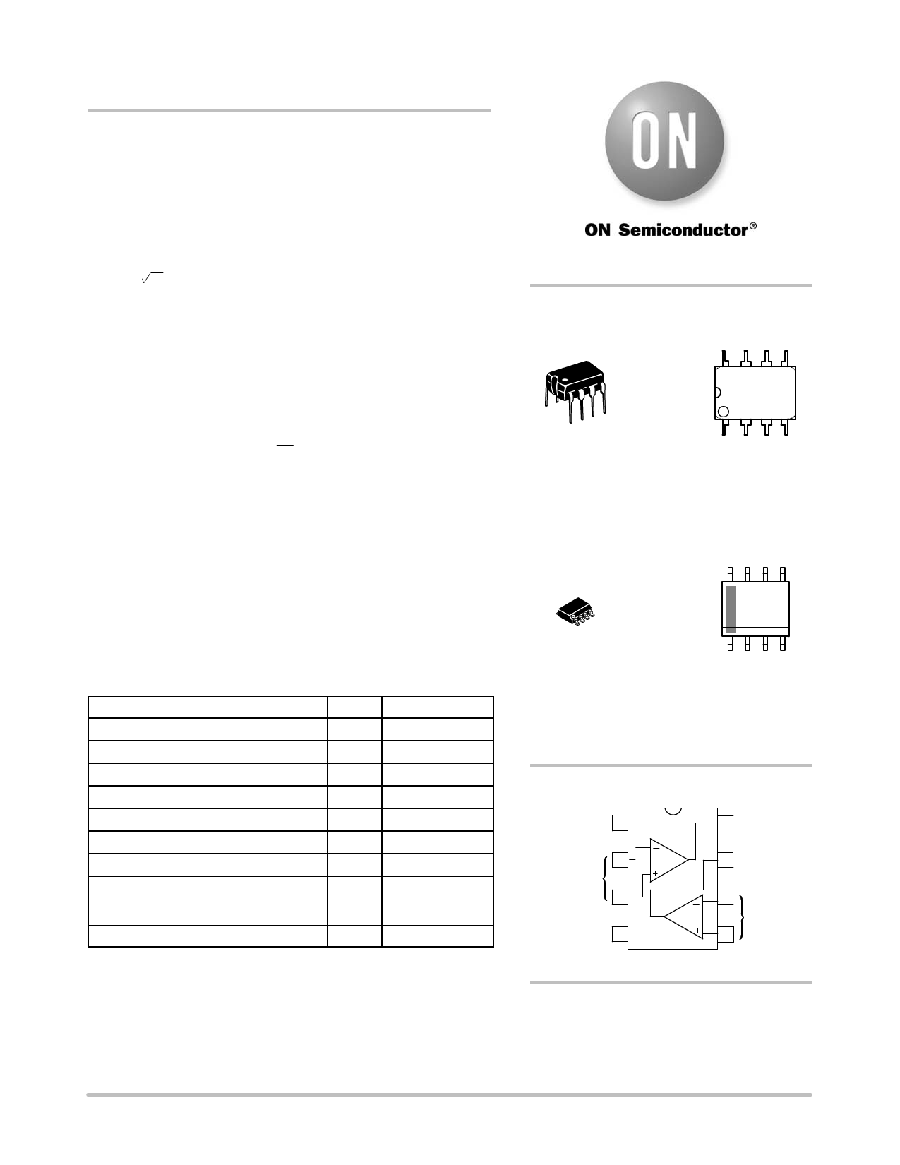
PIN CONNECTIONS
Output 1 1
8 VCC
2
Inputs 1
3
VEE 4
1
2
(Top View)
7 Output 2
6
Inputs 2
5
ORDERING INFORMATION
See detailed ordering and shipping information in the package
dimensions section on page 6 of this data sheet.
© Semiconductor Components Industries, LLC, 2011
1
September, 2011 − Rev. 6
Publication Order Number:
LM833/D
Share Link: 